Method for manufacturing nitride semiconductor wafer or nitride semiconductor device; nitride semiconductor wafer or nitride semiconductor device made by the same; and laser irradiating apparatus used for the same

a technology of nitride semiconductor and semiconductor wafer, which is applied in the direction of solid-state devices, chemical instruments and processes, crystal growth processes, etc., can solve the problems of unsatisfactory surface condition of nitride semiconductor layer, unirradiation of laser beam uniform intensity, and fragments of broken nitride semiconductor layer over disparate substrates, etc., to increase the etching rate of nitride semiconductor, improve the etching rate of chemical

Active Publication Date: 2006-08-24
NICHIA CORP
View PDF11 Cites 35 Cited by
  • Summary
  • Abstract
  • Description
  • Claims
  • Application Information

AI Technical Summary

Benefits of technology

[0013] When the nitride semiconductor is irradiated with light of short wavelength, the nitride semiconductor layer absorbs the light and is heated to a high temperature so as to decompose into nitrogen and metal, while electron-hole pairs are excited in the nitride semiconductor layer so that etching rate of chemical etching becomes very high. Therefore, irradiation of the disparate substrate with a laser beam in an acidic or alkaline etching solution causes the thermal decomposition of the nitride semiconductor layer and the chemical etching to proceed at the same time in the portion being irradiated. This causes the disparate substrate to be lifted off evenly over the entire surface and makes the resultant surface of the nitride semiconductor layer very smooth. As a result, not only the nitride semiconductor layer

Problems solved by technology

When the disparate substrate is removed from the nitride semiconductor layer by irradiating with laser beam, however, there has been such a case as the nitride semiconductor is not fully decomposed in a portion of the wafer, or the nitride semiconductor layer turns into a state of being fused, and a part of the nitride semiconductor layer is broken and lifted off along with the disparate substrate.
Since intensity of the laser beam is distributed in a certain pattern, the wafer is not irradiated with uniform intensity of the laser beam.
As a result, there can occur such a case as the nitride semiconductor is not fully decompose

Method used


Image

  • Method for manufacturing nitride semiconductor wafer or nitride semiconductor device; nitride semiconductor wafer or nitride semiconductor device made by the same; and laser irradiating apparatus used for the same
  • Method for manufacturing nitride semiconductor wafer or nitride semiconductor device; nitride semiconductor wafer or nitride semiconductor device made by the same; and laser irradiating apparatus used for the same
  • Method for manufacturing nitride semiconductor wafer or nitride semiconductor device; nitride semiconductor wafer or nitride semiconductor device made by the same; and laser irradiating apparatus used for the same

Examples


embodiment 1

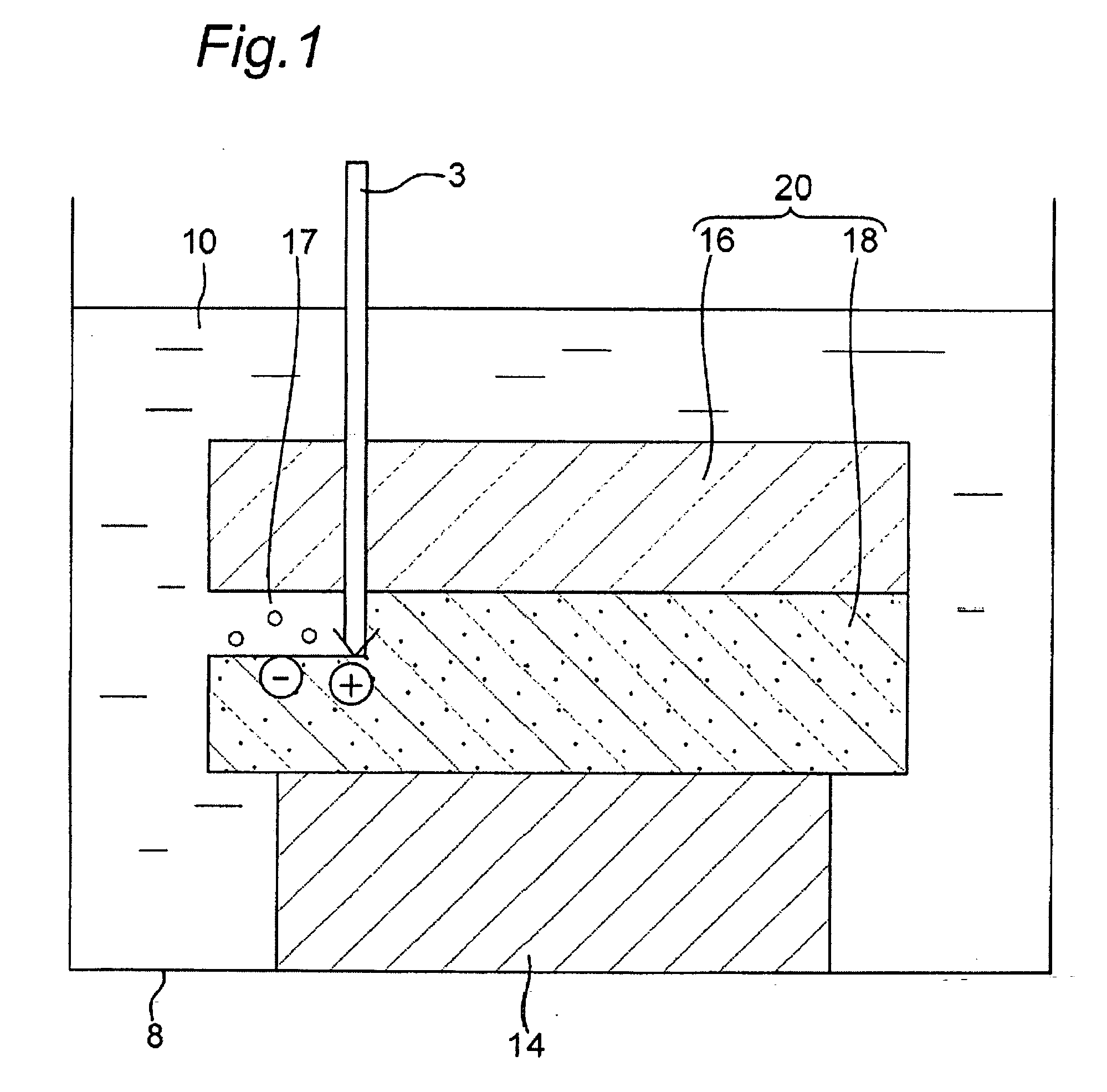
[0029]FIG. 1 is a schematic diagram showing a characteristic portion of the method of manufacturing a nitride semiconductor wafer or a nitride semiconductor device according to the present invention, namely the step of removing a disparate substrate 16 from a wafer 20 whereon a nitride semiconductor layer 18 has been grown on the disparate substrate 16. As shown in FIG. 1, an etching bath 8 contains an acidic or alkaline etching solution 10 in which the wafer 20 is held on a holder 14. The wafer 20 is held so that the disparate substrate 16 faces upward and is irradiated with laser beam 3.

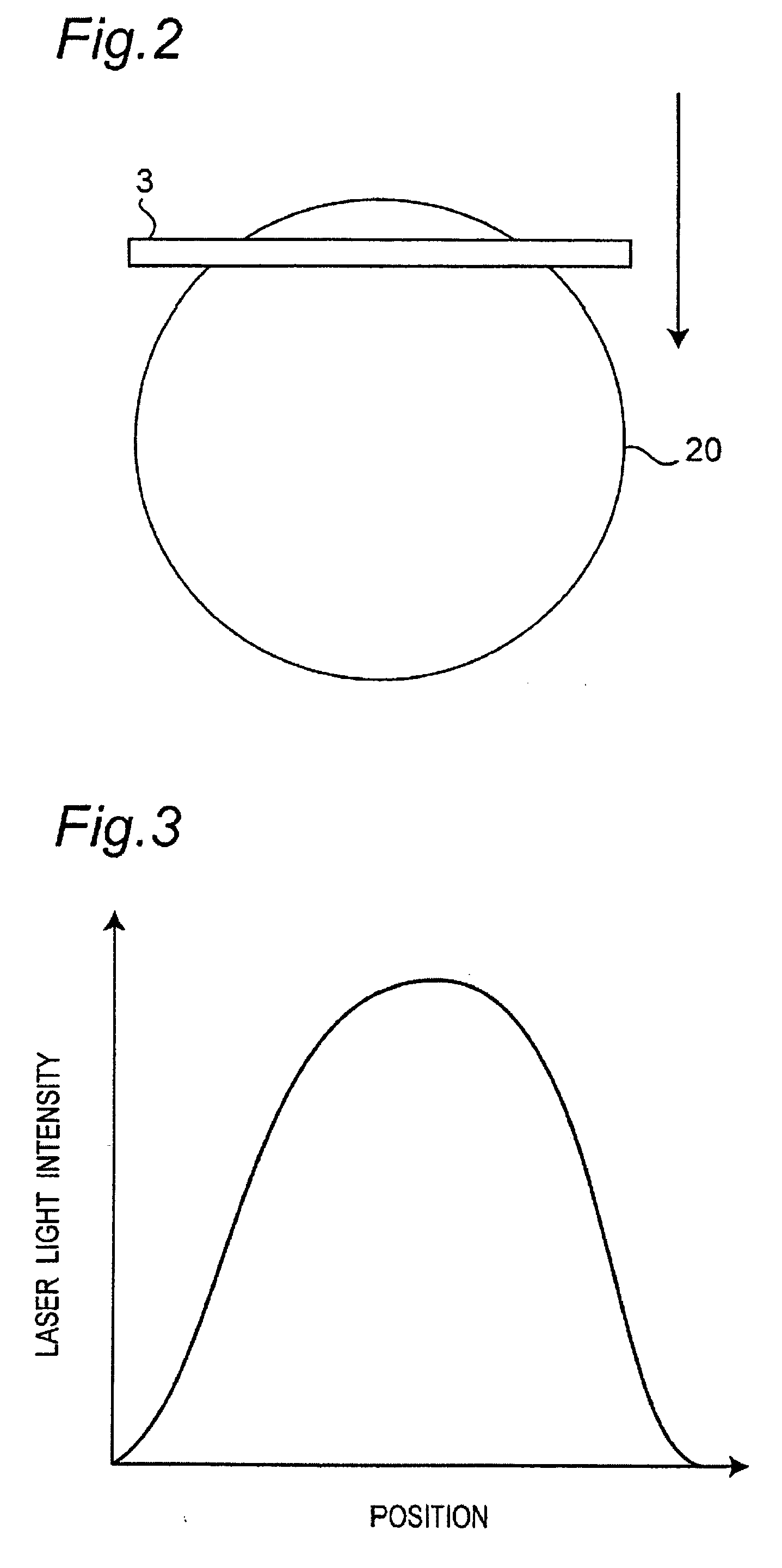
[0030] The laser beam 3 has a linear beam shape as shown in FIG. 2, and is scanned in a direction perpendicular to the longitudinal direction of the beam so as to sweep the entire surface of the wafer 20. Laser beam 3 has a wavelength shorter than the band gap wavelength of the nitride semiconductor layer 18. In case the nitride semiconductor 18 is made of GaN, the laser beam has a wavelength shor...

embodiment 2

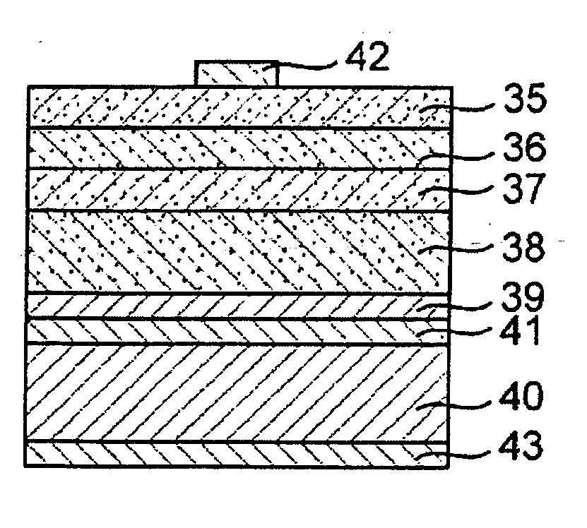
[0045] Now an embodiment where the present invention is applied to the manufacture of an UV light emitting diode or a UV laser as one kind of nitride semiconductor device will be described. A nitride semiconductor device can generally emit light with high internal quantum efficiency by forming a device layer on an underlying layer made of gallium nitride crystal that has been grown at a high temperature on a disparate substrate such as sapphire. In an UV light emitting diode or an UV laser, however, since gallium nitride of the underlying layer has a high absorptivity for ultraviolet rays, emission from the active layer is absorbed by the underlying layer itself, thus resulting in lower external quantum efficiency. For this reason, it has been proposed to, after attaching a support substrate made of Cu—W or the like on the top surface of the wafer on which the device layer has been formed, remove the disparate substrate and further remove the gallium nitride layer that is the underl...

embodiment 3

[0062] Described in this embodiment is an example of manufacturing the nitride semiconductor wafer by a lateral growth process known as the ELOG (epitaxially lateral overgrowth). After forming the nitride semiconductor layer on the disparate substrate by the lateral growth process, the disparate substrate is removed by the method of the present invention, thereby to obtain the nitride semiconductor wafer that is made of the nitride semiconductor only.

[0063] A typical process of lateral growth is one that uses a protective film. For example, a disparate substrate or a nitride semiconductor layer grown thereon is partially covered by a protective film provided thereon. Then the nitride semiconductor is grown through an opening (non-masked region) of the protective film preferentially over the protected portion, or preferably selectively. As patches of the nitride semiconductor that have grown cover the protected portions and coalesce with each other, a film of the nitride semiconduct...


PUM


Abstract

To remove the disparate substrate from nitride semiconductor layer grown over the disparate substrate, that is made of a material different from nitride semiconductor, by irradiating the disparate substrate with laser beam having a wavelength shorter than the band gap wavelength of the nitride semiconductor layer, while supplying an acidic or alkaline etching solution to the interface between the disparate substrate and the nitride semiconductor layer.

Description

BACKGROUND OF THE INVENTION [0001] 1. Field of the Invention [0002] The present invention relates to a method for manufacturing a nitride semiconductor wafer or a nitride semiconductor device, the nitride semiconductor wafer or the nitride semiconductor device obtained thereby and a laser irradiation apparatus used therefor. More particularly, the present invention relates to a method for manufacturing a nitride semiconductor wafer or a nitride semiconductor device that is provided with the step of removing a disparate substrate made of a material different from nitride semiconductor. [0003] 2. Description of the Related Art [0004] When manufacturing a nitride semiconductor wafer or a nitride semiconductor device, it may become necessary to separate nitride semiconductor layer from a disparate substrate that is made of such a material as sapphire or SiC. For example, a nitride semiconductor wafer made of a free-standing nitride semiconductor is generally manufactured by growing a th...

Claims


Application Information

Patent Timeline
IPC IPC(8): H01L21/00C30B11/00H01L21/20H01L33/32
CPCH01L21/30612H01L21/30617H01L21/6835H01L33/0079H01L2221/6835Y10T117/10H01L2924/3025H01L2924/0002Y10S438/94H01L2221/68363H01L2924/00H01L33/0093
Inventor NOGAMI, YOICHI
Owner NICHIA CORP
Why Eureka
Try Eureka