Method for manufacturing a display device with low temperature diamond coatings

a technology of diamond coating and display device, which is applied in the direction of semiconductor devices, organic semiconductor devices, electrical apparatus, etc., can solve the problems of long-term stability problems, high cost, and high cost, and achieves faster operation, high power, and heat-tolerant

Inactive Publication Date: 2006-08-24
CROPPER ANDRE D +1
View PDF40 Cites 15 Cited by
  • Summary
  • Abstract
  • Description
  • Claims
  • Application Information

AI Technical Summary

Benefits of technology

[0031] The present invention has the advantages in that for the first time it is possible to fabricate an OLED display device at a low temperature that is more heat tolerant, that has higher power, that is faster operating, that has longer lifetime, that is bi-directional, that is more resistant to abrasion, and that has higher light conversion efficiency. Such an OLED display device can be fabricated on existing ridged amorphous, poly, continuous-grain or single crystal silicon Thin Film Transistor (TFT) backplanes [1], on the new flexible backplanes using semiconductor or organic TFT [2,3], and on flexible metal or plastic substrates [4,5]. As a result of this new OLED device structure, multiple low temperature diamond layers can be used to create a more efficient, higher power, longer lifetime device for flat panel displays, backlights and flat light sources. References:
[0032] 1. Lih et al., “Full-color active-matrix OLED based on a-Si TFT technology” Journal of the society for Information Display, vol. 11, no. 4, SPEC. ISS., 2003, pp. 617-620.
[0033]2. Afentakis et al. “Polysilicon TFT AM-OLED on thin flexible metal substrates” Proceedings of SPIE—The International Society for Optical Engineering, vol. 5004, 2003, pp. 187-191.
[0034] 3. Troccoli et al., “Amoled TFT pixel circuitry for flexible displays on metal foils” Materials Research Society Symposium—Proceedings, vol. 769, 2003, pp. 93-98.
[0035] 4. Xie et al., “Fabrication of flexible organic top-emitting devices on steel foil substrates” Materials Science and Engineering B: Solid-State Materials for Advanced Technology, vol. 106, no. 3, Feb. 15, 2004, pp. 219-223.
[0036] 5. Chwang et al., “Thin film encapsulated flexible organic Electroluminescent displays”Applied Physics Letters, vol. 83, no. .3, Jul. 21, 2003, p. 413.

Problems solved by technology

However, these diamond samples only have a limited crystal surface area on the order of 1-2 cm2 at the largest and are very expensive to produce.
Thus its applications are very limited.
However, both prior arts used methods to create the boron doped polycrystalline diamond (Moyer) and diamond-like carbon (Kobashi) layers at temperatures above 800° C. and only addressed optimizing the hole side of the OLED display device structure.
Also, the long term stability problem still occurs because the organic layer may undergo re-crystallization, form metal oxide impurities at the metal-organic interface, and other structural change that adversely affect the emissive properties of the device, due to exposure to oxygen or moisture.
However, the organic materials typically used to make OLED display devices are intolerant to temperatures above 200° C. Otherwise a multi-chambered, multi-step process facility would have to be used in which, the diamond drift layer would be created in one apparatus and then transferred to another apparatus to create the OLED display device.
Also since only the cathode is transparent, a bi-directional OLED display device cannot be made from this structure.
However, since the electron and hole mobilities of DLC films are much smaller than those of single crystal or polycrystalline diamond, the light conversion efficiency would be much less than a device made from diamond.
In addition, since either the cathode or anode can be transparent in Jones' patent, a bi-directional OLED display device cannot be made from this structure.
Also, since the thermal conductivity, chemical stability, and impermeability of DLC are greatly inferior to those of diamond such a device would become more susceptible to thermal and moisture damage than a device made from diamond.
None of the above-described processes have sufficiently met this specific need.

Method used


Image

  • Method for manufacturing a display device with low temperature diamond coatings
  • Method for manufacturing a display device with low temperature diamond coatings
  • Method for manufacturing a display device with low temperature diamond coatings

Examples


Embodiment Construction

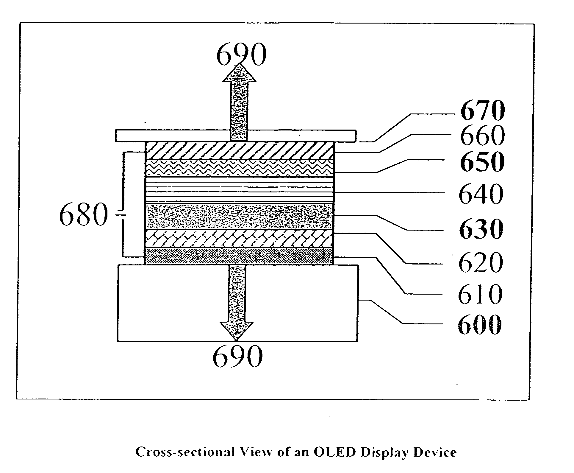
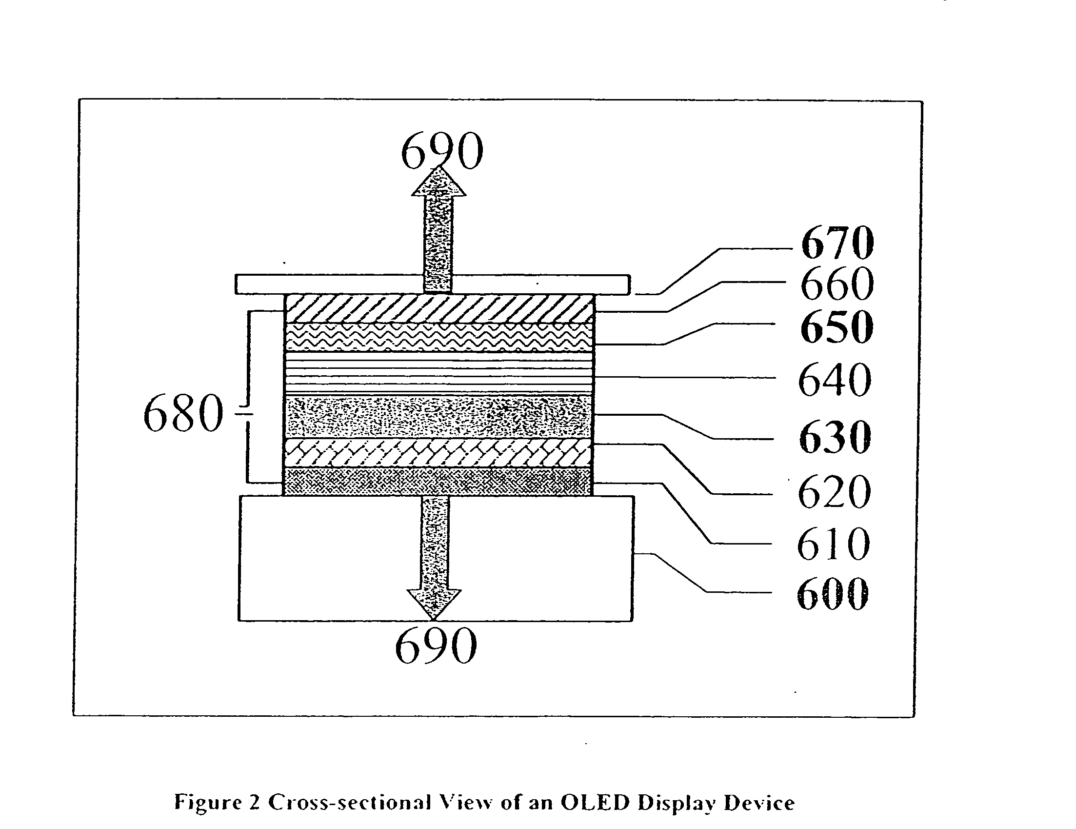
[0045] The present invention relates to an innovative method of fabricating a bi-directional OLED display device with multiple diamond layers deposited by a chemical vapor transport process at temperatures below 750° C. that would significantly increase the light conversion efficiencies and long term reliability and that can be manufactured in a continuous process.

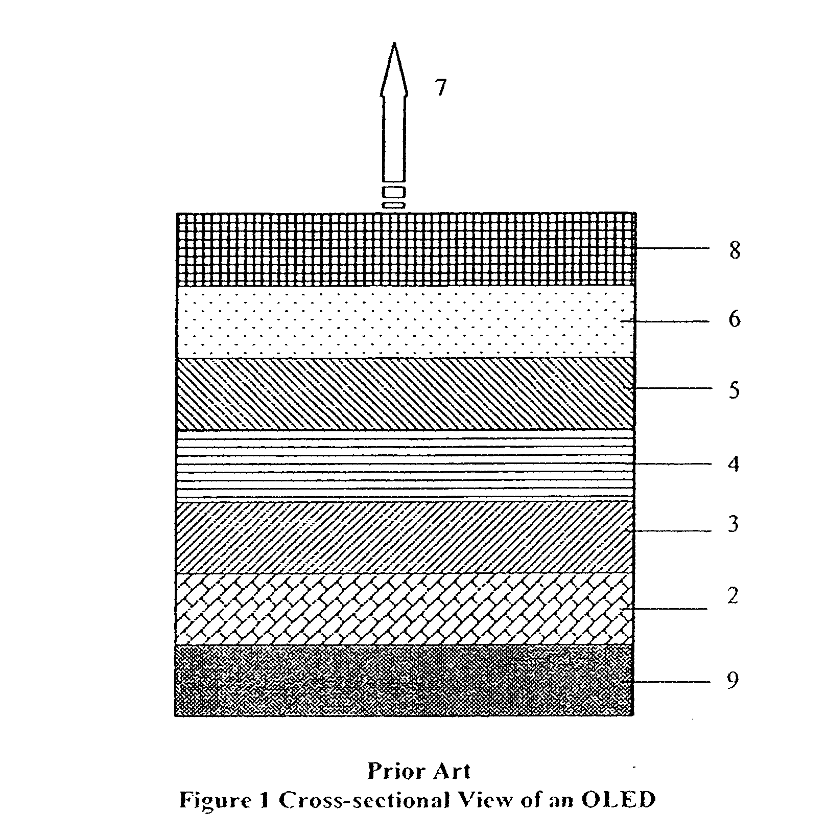
[0046] The performance of OLEDs in display devices has been known to be highly susceptible to degradation by moisture and oxygen. For this reason, it is necessary to limit or control the amount of moisture the organic materials are exposed to, usually by encapsulating the diodes within a metal can or by sandwiching with another glass substrate containing a drying substance, thereby ensuring the continued performance of the OLED as a display. This invention provides for an OLED with transparent thin film encapsulation formed by the low-temperature deposition of diamond onto either a transparent or opaque cathode or anode c...


PUM

PropertyMeasurementUnit
temperatureaaaaaaaaaa
temperaturesaaaaaaaaaa
dielectric constantaaaaaaaaaa

Abstract

A display device with multiple low temperature diamond coatings, including a substrate as a base; an anode layer residing on the diamond substrate for emitting holes; a hole drift layer that includes a doped diamond coating residing on the anode layer; an emissive layer for emitting light and residing on the hole drift layer. The display device also includes an electron transport layer that includes a doped diamond coating residing on the light emitting layer; a cathode layer, residing on the electron transport layer, for emitting electrons that will drift towards the light emitting layer; and a diamond coated encapsulation layer for sealing the display device from atmospheric moisture; wherein the multiple low temperature diamond coatings are all formed below 750° C. on the display device.

Description

CROSS-REFERENCE T RELATED APPLICATIONS [0001] This is a divisonal of application Ser. No. 10 / 897,603, filed on Jul. 23, 2004. [0002] Reference is made to commonly assigned copending application Ser. No. 10 / 897,603, entitled “Method for Manufacturing a Display Device with Low Temperature Diamond Coatings”, which is filed on even date herewith in the names of Andre D. Cropper, and Liya Regel.FIELD OF THE INVENTION [0003] The present invention relates to a display device with multiple diamond coatings deposited by a chemical vapor transport process at temperatures below 750° C. and a method for the manufacture of such a display. This present invention can be used for Organic Light Emitting Diodes (OLED), back lights for Liquid Crystal Displays (LCD), flat light sources, flat panel displays (FPD), etc. BACKGROUND OF THE INVENTION [0004] Organic light emitting devices (OLEDs) have been known for approximately two decades. All OLEDs work on the same general principles. One or more layers ...

Claims


Application Information

Patent Timeline
Patent Type & Authority Applications(United States)
IPC IPC(8): H01L21/00
CPCH01L21/041H01L51/0008H01L51/0096H01L51/5052H01L51/5237H01L51/56H01L2251/5323H10K71/16H10K77/10H10K50/155H10K50/165H10K50/844H10K71/00H10K2102/3031
Inventor CROPPER, ANDRE D.REGEL, LIYA
Owner CROPPER ANDRE D
Why Eureka
Try Eureka