Liquid crystal device and electronic apparatus

a liquid crystal device and electronic equipment technology, applied in the field of liquid crystal devices and electronic equipment, can solve the problems of weakening the regulation force of the alignment control unit at the center area of the pixel electrode, notably lowering the pixel aspect ratio, and effectively disposing of slits

Inactive Publication Date: 2006-09-07
EPSON IMAGING DEVICES CORP
View PDF9 Cites 20 Cited by
  • Summary
  • Abstract
  • Description
  • Claims
  • Application Information

AI Technical Summary

Benefits of technology

[0009] An advantage of some aspects of the invention is that it provides a liquid crystal device which is capable of controlling the alignment of liquid crystal molecules without lowering a pixel opening ratio by effectively disposing slits around an outer periphery of a pixel electrode even when a liquid crystal material having negative dielectric anisotropy is used, and an electronic apparatus having the liquid crystal device.
[0012] According to this aspect, since the liquid crystal layer is made of a liquid crystal material having negative dielectric anisotropy, and an alignment control unit that controls the alignment of the liquid crystal molecules is formed in an area that includes the center of the pixel electrode, at the time of voltage application, the vertically aligned liquid crystal molecules at the center portions of the pixel electrode can be tilted in all directions of 360 degrees, thereby achieving a superior visual angle characteristic. Also, in the case of a polygonal pixel electrode, since the corner portions are spaced apart from the alignment control unit, the regulation force by the alignment control unit at the center area of the pixel electrode becomes weaker. However, according to this aspect, the slits are formed at the corner portions, and the alignment of the liquid crystal molecules is controlled by the distortion in the electric field generated by the slits. Therefore, since the slits are only formed in the areas that are most likely subject to alignment disorder, the alignment of the liquid crystal molecules can be controlled without forming a plurality of slits around the entire outer peripheries of a plurality of pixel electrodes. As a result, as compared with the case in which a plurality of slits are formed around the entire outer peripheries of the pixel electrode, brighter display with a higher pixel aspect ratio can be achieved.
[0015] According to this aspect, since the liquid crystal layer is made of a liquid crystal material having negative dielectric anisotropy and the pixel-electrode is divided into sub-pixels, the vertically aligned liquid crystal molecules can be tilted in a predetermined direction by the oblique electric field at the outer periphery of each of the sub-pixels, thereby achieving a superior visual angle characteristic. In addition, when the pixel electrode is divided into sub-pixels, the sub-pixels are connected to one another via connection portions, and the alignment of the liquid crystal molecules are likely to be subject to alignment disorder at the portion corresponding to the connection portion. However, according to this aspect, since the slits are formed at the outer peripheries of the sub-pixel electrode, extending from both sides of the corresponding pixel electrodes with the connection portions interposed therebetween at sides where the connection portions are located toward centers of the corresponding sub-pixel electrodes, the alignment of the liquid crystal molecules near the connection portion can be efficiently controlled. Therefore, since the slits are only formed in the areas that are most likely subject to alignment disorder, the alignment of the liquid- crystal molecules can be controlled without forming a plurality of slits around the entire outer peripheries of a plurality of pixel electrodes. Therefore, in comparison with the case in which a plurality of slits are formed around the entire outer peripheries of the pixel electrode, brighter display with a higher pixel aspect ratio can be achieved.
[0018] According to this aspect, since the liquid crystal layer is made of a liquid crystal material having negative dielectric anisotropy and the pixel-electrode is divided into sub-pixels, the vertically aligned liquid crystal molecules can be tilted in a predetermined direction by the oblique electric field at the outer periphery of each of the sub-pixels, thereby achieving an superior visual angle characteristics. Also, the pixel electrode is divided into sub-pixel electrodes, each of the sub-pixel electrodes corresponds to a transmissive display region or a reflective display region, and a liquid-crystal-layer thickness adjusting layer is formed on the reflective display region, which makes the thickness of the liquid crystal layer in the reflective display region smaller than the thickness of the liquid crystal layer in the transmissive display region. Therefore, since the difference in retardation (Δn·d) between the transmissive display light and the reflective display light is eliminated, both the transmissive display light and the reflective display light are preferably light-modulated. In this case, a step of the liquid-crystal-layer thickness adjusting layer is located near the interface area between the transmissive display region and the reflective display region, and by the step, the liquid crystal molecules is subject to alignment disorder. However, since oblique slits extend from both side portions located in the interface area between the reflective display region and the transmissive display region toward the center of the sub-pixel electrode, the alignment of the liquid crystal molecules near the interface area between the reflective display region and the transmissive display region can be controlled. Therefore, since the slits are only formed in the areas that are most likely subject to alignment disorder, the alignment of the liquid crystal molecules can be controlled without forming a plurality of slits around the entire outer peripheries of a plurality of pixel electrodes. As a result, as compared with the case in which a plurality of slits are formed around the entire outer peripheries of the pixel electrode, brighter display with a higher pixel aspect ratio can be achieved.
[0019] Preferably, an alignment control unit that controls the alignment of the liquid crystal molecules in the area including each of the centers of the sub-pixel electrodes is preferably formed either on the first substrate or on the second substrate. Through the structure, since the vertically aligned liquid crystal molecules at the center portion of the pixel electrode can be tilted in all directions of 360 degrees, a superior visual angle characteristic can be achieved, and the location of disclination can be fixed, thereby achieving a higher display quality.
[0022] Preferably, the width of each slit is preferably equal to or smaller than 8 μm. If the width of each of the slits exceeds 8 μm, the effect of the oblique electric field generated by the slit becomes excessively large, and there is concern that the liquid crystal molecules of the entire pixel may be subject to alignment disorder. Also, if the width of each of the slits is equal to or smaller than 8 μm, since the alignment of the liquid crystal molecules can be controlled by the oblique electric field generated by the slits, portions corresponding to the silts can be light-modulated, thereby contributing to the display. Therefore, an amount of lost display light can be suppressed to a minimum, and a bright image can be displayed.

Problems solved by technology

However, as disclosed in Non-Patent Document 2, when a plurality of slits are formed around the entire outer peripheries of the sub-pixels, since an area of the slits not directly contributing to the display is large, there is a problem in that a pixel aspect ratio (ratio of portions directly contributing to the display to the entire pixels) may be notably lowered, and thus bright images cannot be displayed.
Also, in the case of a polygonal pixel electrode, since the corner portions are spaced apart from the alignment control unit, the regulation force by the alignment control unit at the center area of the pixel electrode becomes weaker.
In addition, when the pixel electrode is divided into sub-pixels, the sub-pixels are connected to one another via connection portions, and the alignment of the liquid crystal molecules are likely to be subject to alignment disorder at the portion corresponding to the connection portion.
If the width of each of the slits exceeds 8 μm, the effect of the oblique electric field generated by the slit becomes excessively large, and there is concern that the liquid crystal molecules of the entire pixel may be subject to alignment disorder.

Method used


Image

  • Liquid crystal device and electronic apparatus
  • Liquid crystal device and electronic apparatus
  • Liquid crystal device and electronic apparatus

Examples


first embodiment

General Structure

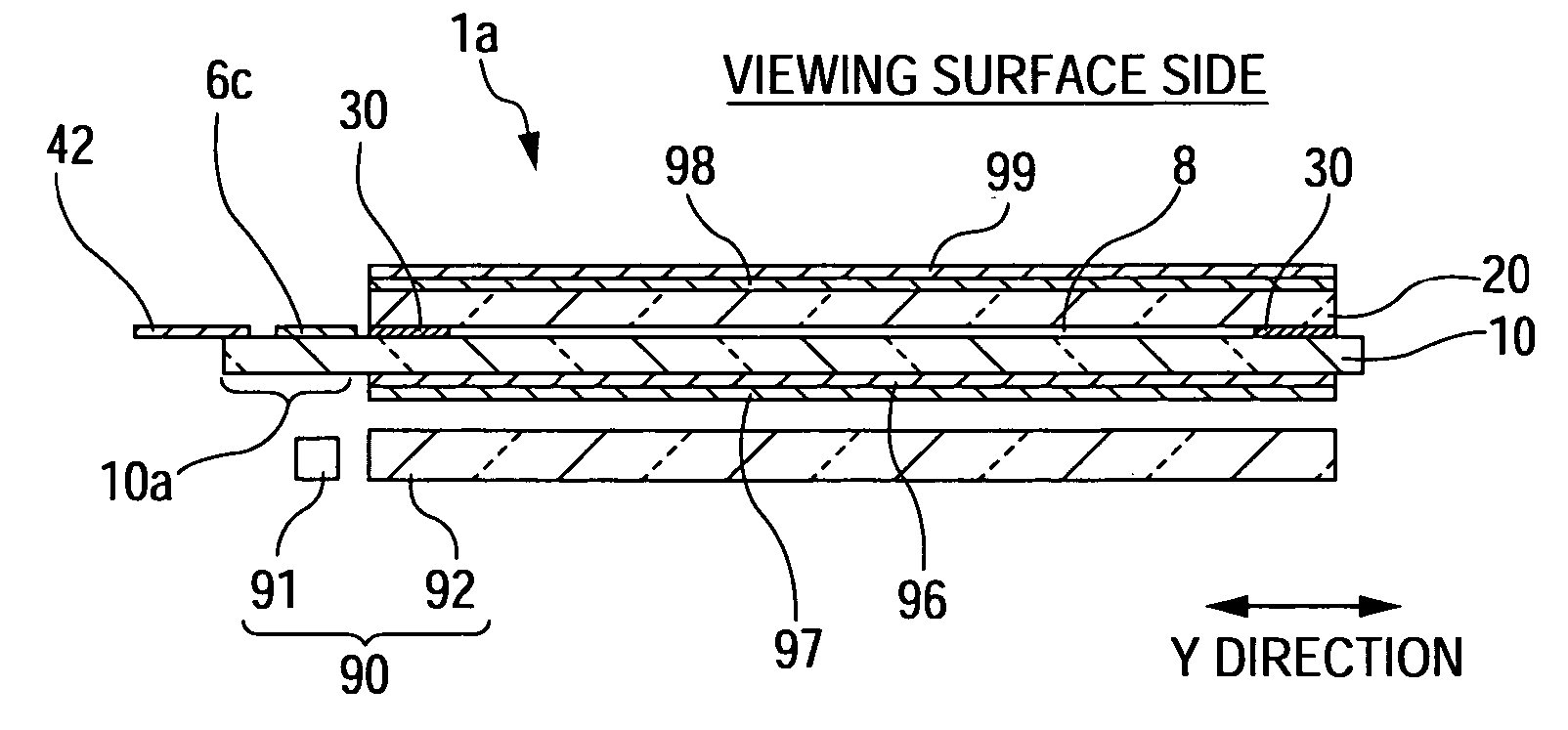
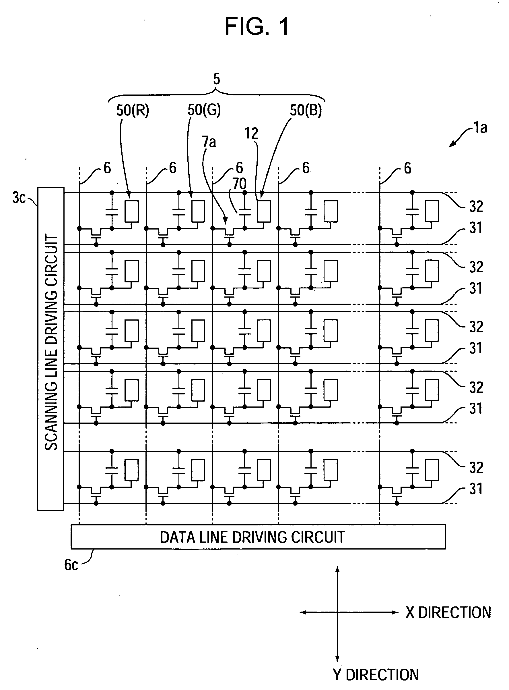
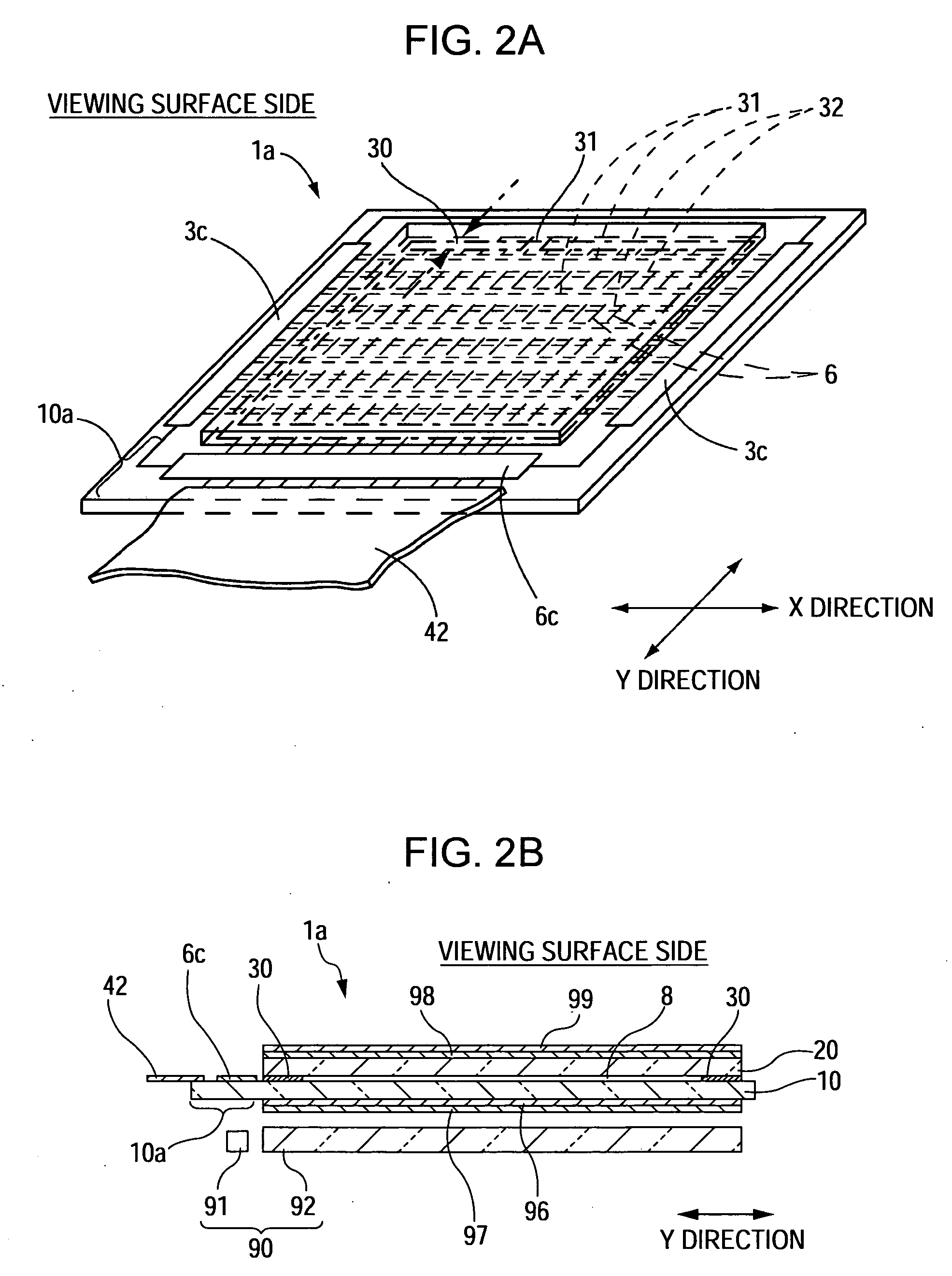
[0043]FIG. 1 is a block diagram illustrating an electrical structure of a liquid crystal device according to a first embodiment of the invention. FIG. 2A is a schematic perspective view of the liquid crystal device according to the first embodiment of the invention viewed from an oblique upside (counter substrate), and FIG. 2B is a diagram schematically illustrating a cross section of the liquid crystal device according to the first embodiment of the invention cut in a Y direction. It is noted that since the liquid crystal device according to the present embodiment is one for color display and thus pixels correspond to a red light component (R), a green light component (G), and a blue light component (B), reference numerals (R), (G), and (B) are affixed to the pixels corresponding to the respective colors.

[0044] The liquid crystal device 1a shown in FIG. 1 is a transmissive active-matrix-type liquid crystal device using thin film transistors (hereinafter, referre...

second embodiment

[0058]FIG. 5 is a plan view schematically illustrating a structure of a pixel corresponding to a single dot of a liquid crystal device according to a second embodiment of the invention. FIG. 6 is an enlarged cross-sectional view illustrating one of a plurality of pixels formed in the liquid crystal device according to the second embodiment of the invention, and corresponds to a cross-sectional view taken along the line VI-VI of FIG. 5. FIGS. 7A and 7B are diagrams illustrating equipotential lines when slits are formed in a sub-pixel electrode in the liquid crystal device according to the second embodiment of the invention. In addition, since a basic structure of the liquid crystal device according to the second embodiment is the same as that of the first embodiment, and the same constituent elements are denoted by the same reference numerals, and the description thereof will be omitted.

[0059] As in the first embodiment, the liquid crystal device 1a shown in FIGS. 5 and 6 is a trans...

third embodiment

[0072]FIG. 8 is a plan view schematically illustrating a structure of a pixel corresponding to a single dot of a liquid crystal device according to a third embodiment of the invention. FIG. 9 is an enlarged cross-sectional view illustrating one of a plurality of pixels formed in the liquid crystal device according to the third embodiment of the invention, and corresponds to a cross-sectional view taken along the line IX-IX of FIG. 8. Since a basic structure of the liquid crystal device according to the present embodiment is the same as that of the first embodiment, the same constituent elements are denoted by the same reference numerals, and the description thereof will be omitted.

[0073] Differently from the first embodiment, the liquid crystal device 1a shown in FIGS. 8 and 9 is a transflective active-matrix-type liquid crystal device. A reflective layer 16 made of aluminum alloy, silver alloy, or the like is formed on the inner surface of the element substrate 10 in a region, whi...


PUM

PropertyMeasurementUnit
widthaaaaaaaaaa
heightaaaaaaaaaa
lengthaaaaaaaaaa

Abstract

A liquid crystal device includes a first substrate that has an inner surface on which a pixel electrode is formed; a second substrate that has an inner surface on which a counter electrode constituting a pixel is formed opposite to the pixel electrode; and a liquid crystal layer that is held between the first substrate and the second substrate and has negative dielectric anisotropy. In addition, an alignment control unit for controlling the alignment of the liquid crystal molecules is formed in an area including the center of the pixel electrode on either the first substrate or the second substrate; and the pixel electrode has an approximately polygonal shape, and slits extending from an outer periphery toward the center are formed at corner portions of the pixel electrode.

Description

RELATED APPLICATIONS [0001] This application claims priority to Japanese Patent Application No. 2005-58470 filed Mar. 3, 2005 which is hereby expressly incorporated by reference herein in its entirety. BACKGROUND [0002] 1. Technical Field [0003] The present invention relates to a liquid crystal device using liquid crystal having negative dielectric anisotropy, and to an electronic apparatus having the liquid crystal device. [0004] 2. Related Art [0005] Generally, an active-matrix-type liquid crystal device includes a first substrate that has an inner surface on which a pixel electrode is formed, a second substrate that has an inner surface on which a counter electrode constituting a pixel is formed opposite to the pixel electrode, and a liquid crystal layer that is held between the first substrate and the second substrate. In such a liquid crystal device, as a technology for improving a visual angle characteristic, a technology adopting a VA (vertical alignment) mode in which liquid...

Claims


Application Information

Patent Timeline
Patent Type & Authority Applications(United States)
IPC IPC(8): G02F1/1335
CPCG02F1/1393G02F1/133707G02F1/134309B42F13/14
Inventor KURASAWA, HAYATO
Owner EPSON IMAGING DEVICES CORP
Why Eureka
Try Eureka