Surface plasmon resonance sensor with high sensitivity
a surface plasmon resonance and sensor technology, applied in the field of high-sensitivity surface plasmon resonance (spr) sensors, can solve the problems of limited capability, sensitivity of the spr sensor available until now is far from satisfaction with low-concentration detection of analytes, and achieves enhanced detecting sensitivity, high sensitivity, and enhanced the effect of surface electromagnetic radiation
- Summary
- Abstract
- Description
- Claims
- Application Information
AI Technical Summary
Benefits of technology
Problems solved by technology
Method used
Image
Examples
example 1
Surface Plasmon Resonance (SPR) Sensor with High Sensitivity
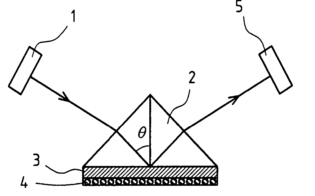
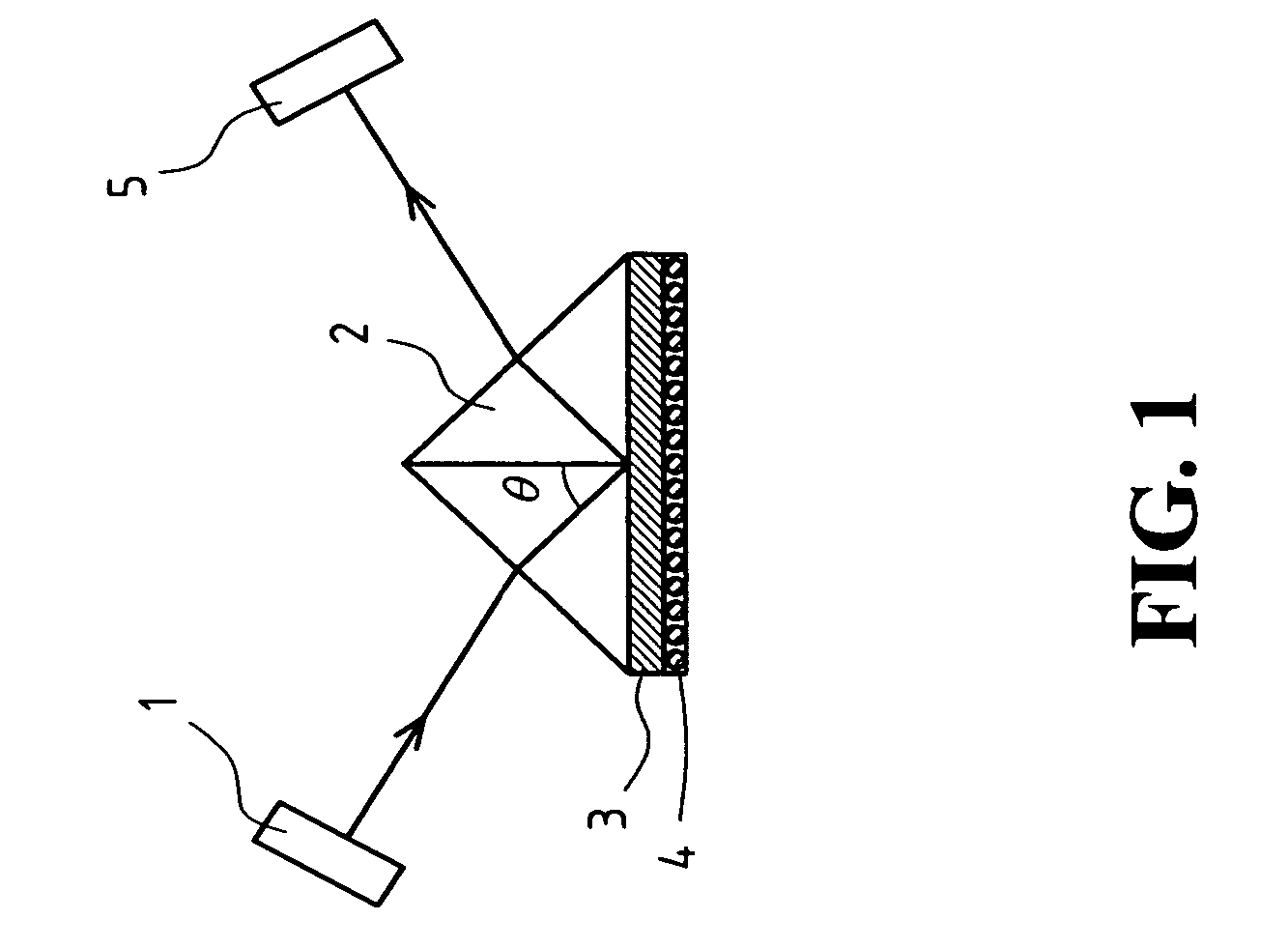
[0031] As indicated in FIG. 1, a SPR sensor comprises an incident light source (1), a prism (2), a metallic layer (3), a layer of metallic nanoparticle layer (4), and a light detector (5).
[0032] The metallic layer (3) having a thickness of about 50 nm is formed on a surface of the prism (2) by way of for example RF magnetron sputtering method for precisely controlling the film thickness thereof, or alternatively, by co-sputtering or vapor-plating method generally employed to form metallic films. The material adopted for the metallic layer (3) is gold or silver.
[0033] The layer of metallic nanoparticle (4) having a thickness of 1-50 nm is formed on the metallic layer (3) by way of RF magnetron sputtering method using dielectric substance and the metal for creating metallic nanoparticles as the target for being mixedly deposited on the metallic layer (3) to form the metallic nanoparticle layer. Alternatively, the solution ...
example 2
Enhanced Raman Scattering Spectra of Metallic Nanoparticles
[0036] After different configurations including sliver layer, silver nanoparticle layer, and monolayer of crystal violet are coated on different prisms in sequence from the bottom to the top thereof to form respective test specimens: [0037] (A) Prism (glass), metallic layer (silver layer), metallic nanoparticle layer (silver nanoparticle layer), and then monolayer of crystal violet; [0038] (B) Prism (glass), metallic nanoparticles (silver nanoparticles), and then monolayer of crystal violet; [0039] (C) Prism (glass), metallic layer (silver layer), mono-layer of crystal violet, and then metallic nanoparticles layer (silver nanoparticles); and [0040] (D) Prism (glass), metallic layer, and then monolayer of crystal violet.
[0041] Different patterns of Raman scattering can be observed as shown in FIG. 3. When compared with each other, the configuration of specimens A, B, and C containing a silver nanoparticle layer are all foun...
example 3
Comparison of SPR Sensors Having Respective Layer Structures
[0042] Different layer structures formed on SPR sensors according to the method described in example 1 from the bottom to the top of prisms are listed below as: [0043] (A) Prism (glass), then a metallic layer (golden layer); [0044] (B) Prism (glass), metallic layer (golden layer), then, dielectric layer (silicon dioxide layer); [0045] (C) Prism (glass), metallic layer (golden layer), then, metallic nanoparticle layer (gold nanoparticle layer); and [0046] (D) Prism (glass), metallic layer (golden layer), metallic nanoparticle layer, then, dielectric layer (silicon dioxide layer).
[0047] After different films are coated on respective SPR sensor, water, as an analyte, is flowed through the surface of the SPR sensor for measuring respective reflectivity. As indicated in FIG. 4—plotted curves of spectra based on different incident angle vs. reflectivity of SPR sensor—the metallic nanoparticle layer has significantly expanded th...
PUM
| Property | Measurement | Unit |
|---|---|---|
| thickness | aaaaa | aaaaa |
| diameter | aaaaa | aaaaa |
| thickness | aaaaa | aaaaa |
Abstract
Description
Claims
Application Information


