

Method of manufacturing semiconductor memory having capacitor of high aspect ratio to prevent deterioration in insulating characteristics
a semiconductor memory and high aspect ratio technology, applied in the direction of semiconductor devices, capacitors, electrical devices, etc., can solve the problems of reducing the amount of charge storage in the capacitor, raising the aspect ratio of the connection plug having a high aspect ratio, and preventing the deterioration of the characteristic of the capacitor. , to achieve the effect of high aspect ratio and preventing the deterioration of the capacitor
- Summary
- Abstract
- Description
- Claims
- Application Information
AI Technical Summary
Benefits of technology
Problems solved by technology
Method used
Image

Examples
first embodiment
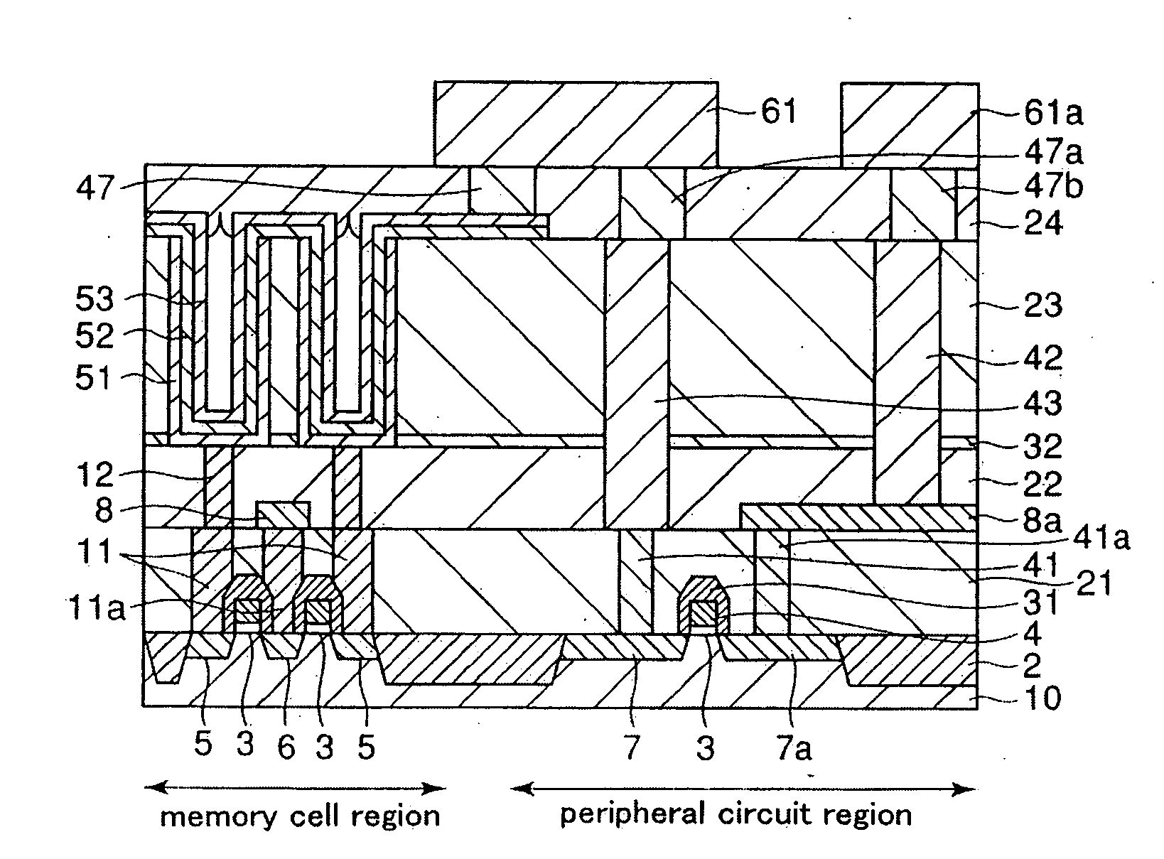
[0041] Explanations will be given of the configuration of semiconductor memory according to the first embodiment of the present invention. FIG. 14 is a sectional view showing a configuration example of a semiconductor memory according to the first embodiment.
[0042] As shown in FIG. 14, the semiconductor memory of the first embodiment is provided with a peripheral circuit region where connection plugs 42, 43 are connected to second layer wirings 61, 61a through connection plugs 47a, 47b.
[0043] Next, the method of manufacturing the semiconductor memory according to the first embodiment of the present invention will be explained with reference to FIG. 15 to FIG. 25.
[0044] First, similar to the conventional example, isolation insulating film 2, gate oxide film 3, gate electrode 4, diffusion layer regions 5, 6, 7, 7a, polysilicon plugs 11, 11a, metal plugs 41, 41a, bit line 8, first layer wiring 8a, interlayer insulating films 31, 22, polysilicon plug 12, and interlayer insulating fil...
second embodiment
[0054] A difference between the second embodiment and the first embodiment is that one interlayer insulating film is added after metal plugs 42, 43 are formed to prevent the film of the lower electrode and the metal plugs from coming into contact and reacting. In this embodiment, even if a polysilicon film is used as the lower electrode and a metal plug includes a tungsten film, it is possible to avoid problems in which, because of the reaction of both and the formation of tungsten silicide, the resistance values of the metal plugs are raised and abnormal growth occurs during formation of polysilicon.
[0055] Next, the method of manufacturing a semiconductor memory having a capacitor of the MIM type according to the second embodiment of the present invention will be explained with reference to FIG. 26 to FIG. 35.
[0056] First, similar to the first embodiment, isolation insulating film 2, gate oxide film 3, gate electrode 4, diffusion layer regions 5, 6, 7, 7a, polysilicon plugs 11, 1...
third embodiment
[0059] The third embodiment shows the example for applying this invention to a capacitor having a lower electrode of a pedestal (pillar) structure. The method of manufacturing the semiconductor memory according to the third embodiment of the present invention will be explained with reference to FIG. 36 to FIG. 45.
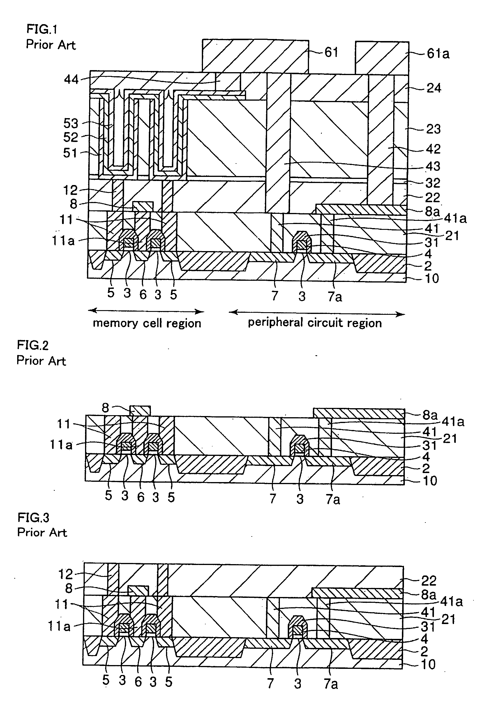
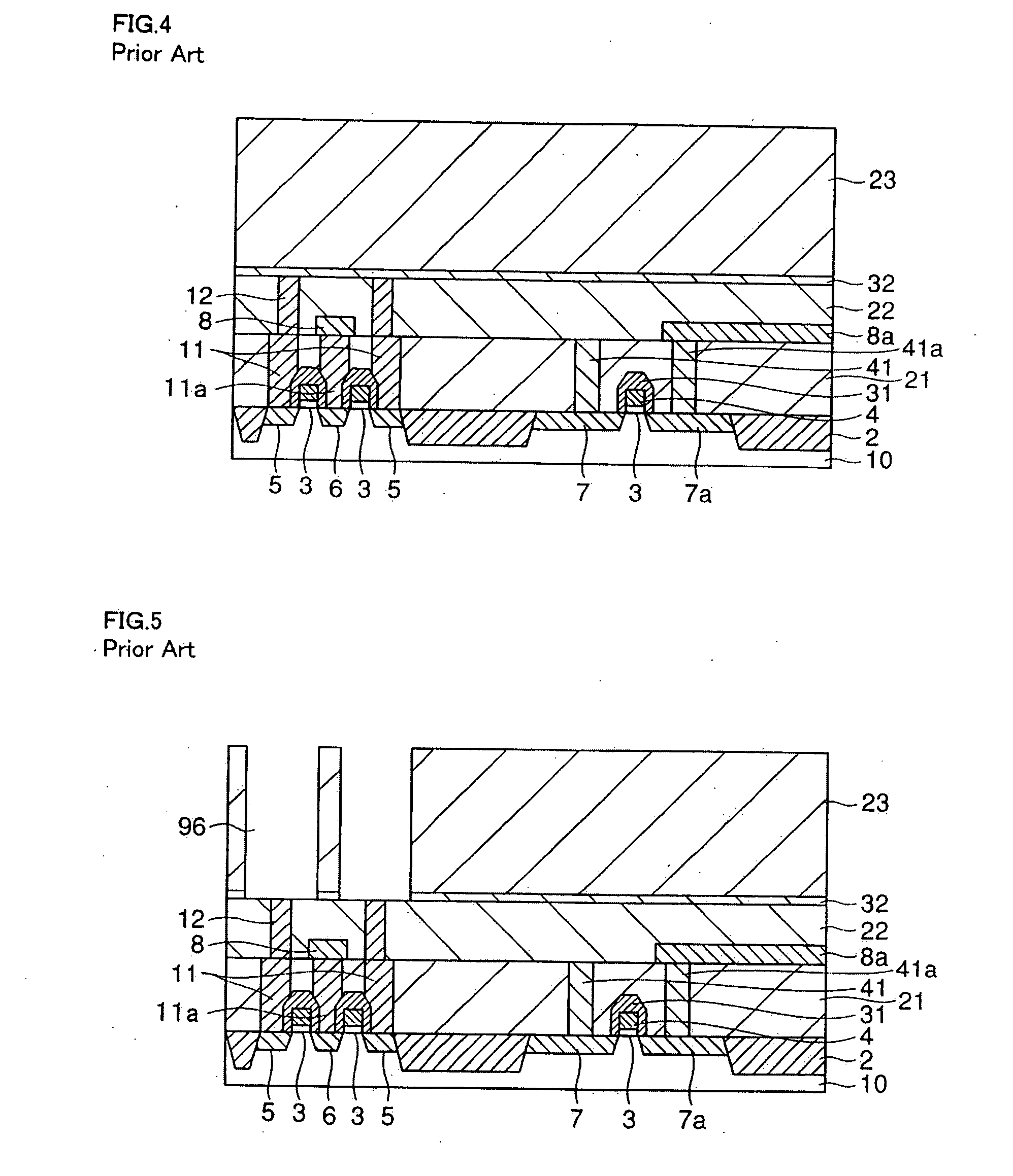
[0060] First, similar to the conventional example, isolation insulating film 2, gate oxide film 3, gate electrode 4, diffusion layer regions 5, 6, 7, 7a, polysilicon plugs 11, 11a, metal plugs 41, 41a, bit line 8, first layer wiring 8a, interlayer insulating film, 22, polysilicon plug 12, and interlayer insulating films 32, 23 are formed sequentially (refer to FIG. 4). Successively, cylinder hole 96 that penetrates interlayer insulating films 23, 32 is formed, and the surface of polysilicon plug 12 is exposed to the bottom of cylinder hole 96. On the other hand, connection holes 92, 93 that penetrates interlayer insulating films 23, 32, 22 are formed, and the surfaces of f...
PUM
 Abstract
Description
Claims
Application Information