System and method for multiple bit optical data transmission in memory systems

a memory system and optical data technology, applied in the field of memory systems, can solve the problems of memory latency, the response time of computer memory systems has not kept up with the increase in microprocessor speed, and other aspects of computer design and manufacture, so as to increase the speed at which data is transmitted, increase the bandwidth of optical transmission media, and carry more data more quickly

Inactive Publication Date: 2006-09-14
MICRON TECH INC
View PDF99 Cites 46 Cited by
  • Summary
  • Abstract
  • Description
  • Claims
  • Application Information

AI Technical Summary

Benefits of technology

[0012] The system and method of the present invention increases the speed at which data can be communicated in memory systems using optical transmission media. The present invention uses an optical transmitter operable to emit optical signals comprising a plurality of wavelengths of light. One example of such an optical transmitter would be a light emitting diode having a composite bond pad comprised of sections of chemically different materials, each of which generates light at different wavelengths. Each section of the optical transmitter would have a separate input so that each section could be selectively, separately activated. As a result, pulses generated by the optical transmitter comprise light of one wavelength or a number of different wavelengths. Consequently, each pulse of the optical transmitter of the present invention can represent more than a single bit of data. Receiving the signal is a photoreceptor having sections of chemically different materials corresponding to the composition of the materials used in the optical transmitter. The sections of the photoreceptor react to the light of different wavelengths generated by the sections optical transmitter, with each section of the

Problems solved by technology

With improvements in semiconductor miniaturization and manufacturing, today's microprocessors operate at gigahertz clock speeds, while other aspects of computer design and manufacture have not kept pace.
As a result, a microprocessor may run at gigahertz speeds, but be left sitting idle waiting on the computer's subsystems to respond to instructions or return data.
To name one very significant example, the response time of computer memory systems has not at all kept up with increases in microprocessor speed.
“Memory latency,” i.e., delays in responding to processor requests for data, is a large problem.
Moreover, the disparity between the speed of processor clocks and memory clocks is growing.
Further compounding the problem is the fact that a memory system may require ten or more of its own memory clock cycles to respond to a memory retrieval request, thus, the ratio for a complete memory cycle is far worse.
Today, completion of one full memory cycle may result in the waste of hundreds of processing cycles.
In the near future, based on current performance trends in microprocessors, completion of a memory cycle may result in the waste of thousands of processing cycles.
Although memory latency results in part from the slower speed

Method used


Image

  • System and method for multiple bit optical data transmission in memory systems
  • System and method for multiple bit optical data transmission in memory systems
  • System and method for multiple bit optical data transmission in memory systems

Examples


Embodiment Construction

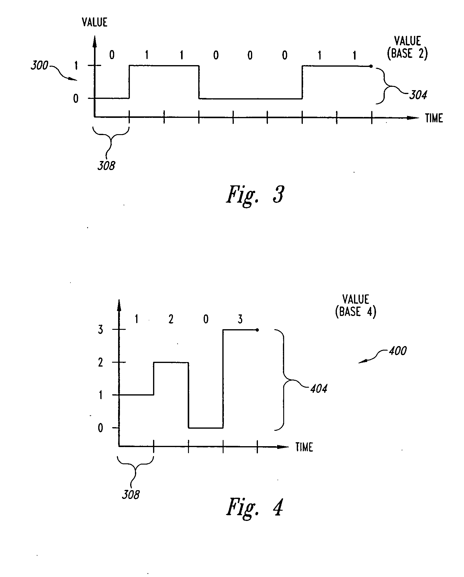
[0025] Instead of communicating bits of data using conventional, conductive signal lines, embodiments of the present invention communicate bits of data using light. In particular, embodiments of the present invention use optical transmitters and receivers which are capable of generating and deciphering, respectively, compound light signals comprising signals having a plurality of wavelengths. The compound signals allow for each light signal to represent multiple bits of data, effectively increasing the bandwidth of the optical data transmission system.

[0026]FIG. 3 is a graph 300 of an example binary signal 304 generated by a monochromatic LED or other light source. In the example of FIG. 3, the signal 304 being sent represents the number “99.” A conventional LED would transmit this number in binary, base two form, which could be transmitted in a single, eight-bit data byte as “01100011.” The graph 300 shows this signal 304 sent over time. The unit of time 308 marked in FIG. 3 is th...


PUM


Abstract

The disclosed system and method data increases data transmission speed through a memory system by using optical signals comprising a plurality of wavelengths of light so that each pulse of optical signals can represent more than a single bit of data. An optical transmitter comprises multiple, separately controllable light-emitting sections which generate light at different wavelengths. A photoreceptor, comprising sections of materials responsive to light received at different wavelengths, provides an output signal corresponding to the light signals received at the different wavelengths. The photoreceptor therefore can decode the received optical signals into a multiple bit output sequence corresponding with the multiple bit sequence originally transmitted. The disclosed method and system can be used to communicate signals between a plurality of memory devices and a memory hub within a memory module or directly to a system memory controller, and/or between a plurality of memory hubs and a system memory controller.

Description

TECHNICAL FIELD [0001] The present invention is directed to memory systems. More particularly, the present invention is directed to increasing the speed of data transmission in a memory system by using optical data transmission to simultaneously transmit multiple data bits. BACKGROUND OF THE INVENTION [0002] The underlying technology and benefits of optical data transmission and fiber optic technology are well known in the art and beyond. Signals in the form of light, at wavelengths both within and beyond the visible spectrum, can be transmitted through free space, a reflective wave guide such as a fiber optic medium, or similar means. Whatever medium is. used, the potential bandwidth is tremendous. Moreover, as compared to electrical signals transmitted through conventional conductive wiring, problems with noise, crosstalk, and similar concerns are reduced if not eliminated. It is no surprise, therefore, that fiber optic cabling has been replacing conventional conductive cabling as...

Claims


Application Information

Patent Timeline
IPC IPC(8): H04B10/00
CPCH04B10/801
Inventor MURPHY, TIM
Owner MICRON TECH INC
Why Eureka
Try Eureka