Method for enhancing homogeneity and effeciency of carbon nanotube electron emission source of field emission display

a carbon nanotube and electron emission source technology, applied in the manufacture of electrode systems, liquid/fluent solid measurements, electric discharge tubes/lamps, etc., can solve the problems of reducing the efficiency of carbon nanotubes, limiting the manufacturing cost and cubic structure, and unable to achieve homogeneity of large-scale electron emission sources. , to achieve the effect of enhancing the electron conductivity of carbon nanotubes and the cathode electron layer

Inactive Publication Date: 2006-09-28
TECO NANOTECH CO LTD
View PDF6 Cites 5 Cited by
  • Summary
  • Abstract
  • Description
  • Claims
  • Application Information

AI Technical Summary

Benefits of technology

[0008] The present invention is to provide a method to overcome the drawbacks in the conventional arts described above. The present invention employs electrophoresis deposition technology to manufacture the electron emission source of the field emission display. In the present invention, the carbon nanotube powder made from arch discharge is used to prepare the electrophoresis solution. In addition, some proper chargers are used, rendering the electrolyte ions to produce good ionic distribution effect. This can enhance the distribution properties of carbon nanotubes in the water or alcoholic electrophoresis solution. The homogeneity of electrophoresis deposition on the surface of cathode electrode is thus enhanced. In addition, the properly selected charger forms conductive metallic salt oxide during the baking process after the electrophoresis deposition process, which will enhance the electron production efficiency of the carbon nanotube electron emission source layer.
[0011] After the deposition process of the cathode structure is completed, the combination is baked with a low temperature so as to remove the residual alcoholic solution on the cathode structure. Meanwhile, the indium chloride charger and the electrolyte hydroxide ions react to form indium hydroxide. Next, a sintering process is performed for re-oxidating the indium hydroxide on the cathode electrode layer back to indium oxide. Consequently, the electron conductivity of the carbon nanotubes and the cathode electron layer is enhanced.

Problems solved by technology

However, there are still limitations of the manufacturing cost and the cubic structure for fabricating the carbon nanotubes on each pixel of the cathode electrode structure, according to the electron emission source structure of the triode field emission display described above.
In particular, the homogeneity of large size electron emission source is even harder to achieve.
Since the magnesium oxide is not a good conductor, although the weighted concentration thereof in the electrophoresis process is generally controlled to be below 0.1%, which does not affect the efficiency for generating electron beams from the carbon nanotube electron emission layer, it does not enhance the efficiency, either.

Method used


Image

  • Method for enhancing homogeneity and effeciency of carbon nanotube electron emission source of field emission display
  • Method for enhancing homogeneity and effeciency of carbon nanotube electron emission source of field emission display
  • Method for enhancing homogeneity and effeciency of carbon nanotube electron emission source of field emission display

Examples


Embodiment Construction

[0017] In order to better understanding the features and technical contents of the present invention, the present invention is hereinafter described in detail by incorporating with the accompanying drawings. However, the accompanying drawings are only for the convenience of illustration and description, no limitation is intended thereto.

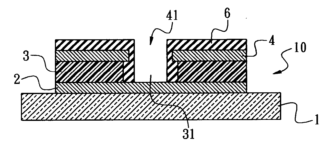
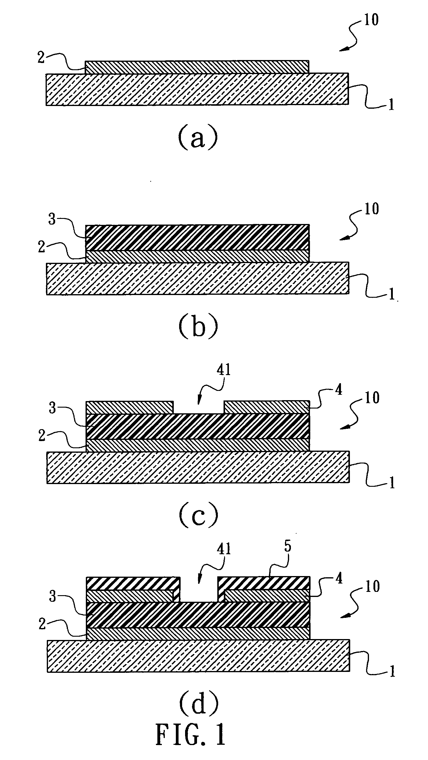
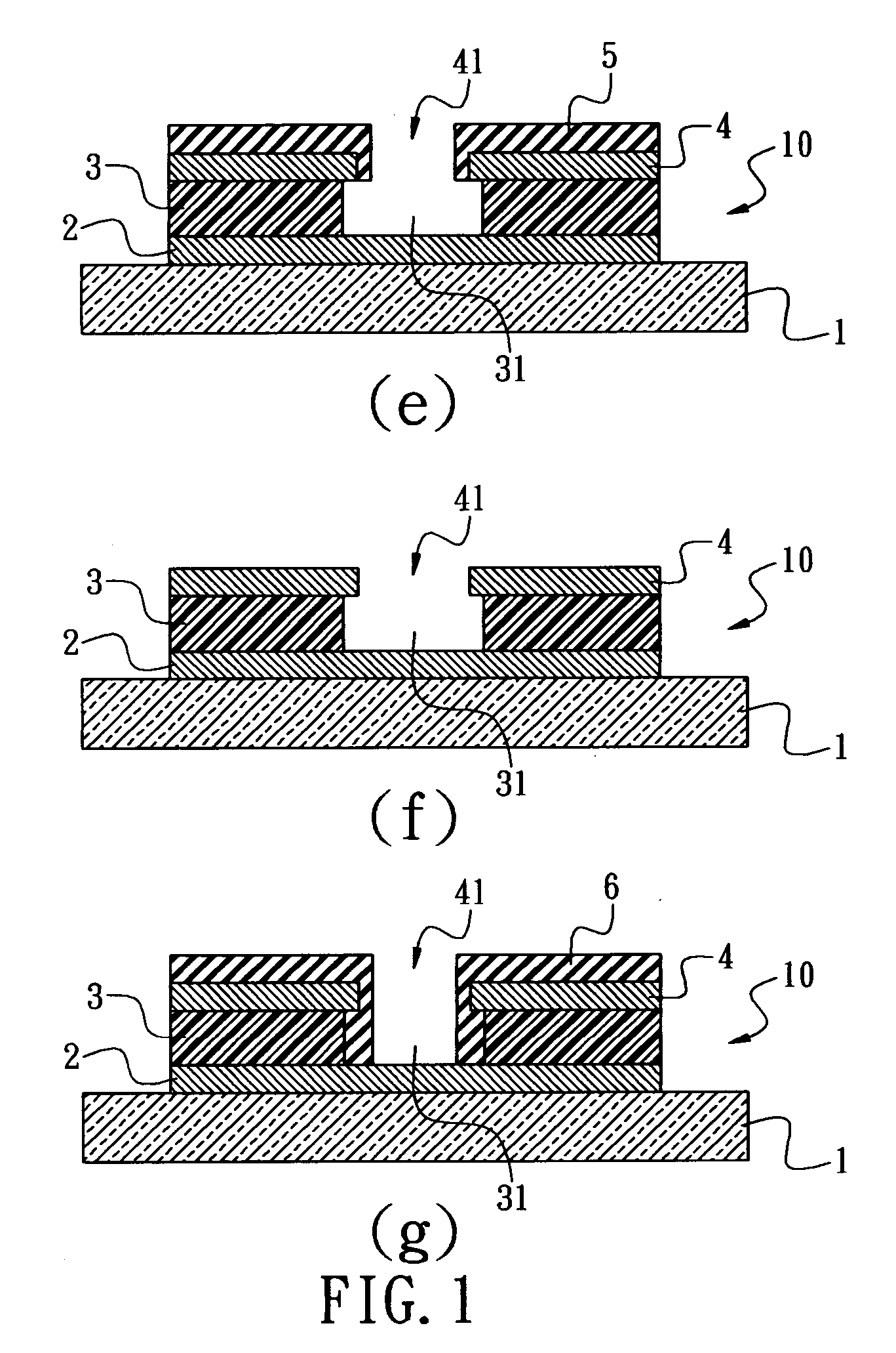
[0018] Referring to FIG. 1(a) to FIG. 1(g), a process for manufacturing a semi-manufactured cathode structure, in accordance with the present invention, is illustrated. As shown, the method of the present invention for enhancing the efficiency and the homogeneity of carbon nanotube electron emission source manufactured by means of electrophoresis deposition employs some proper charger to manufacture the carbon nanotube electron emission source, thereby improving the homogeneity of carbon nanotubes deposited on the surface of the cathode structure 10.

[0019] In the beginning, a cathode electrode layer 2 is formed on the surface of a glass substrate 1...


PUM

PropertyMeasurementUnit
electric fieldaaaaaaaaaa
diameteraaaaaaaaaa

Abstract

A method for enhancing the homogeneity and efficiency of carbon nanotube electron emission source. The method includes the following steps. First, a semi-manufactured cathode structure is prepared. Then, the cathode structure and the metallic plate are connected to the electrophoresis electrodes. After that, the side of the cathode structure to be electrophoresis deposited is kept a fixed distance in parallel with the metallic plate. Then, the electrophoresis deposition is performed to the semi-manufactured cathode structure by placing the combination into the solution of the electrophoresis tank. Later, an electric field is formed from a direct current voltage of a power supply. In this manner, the carbon nanotubes are deposited on the cathode electrode to form the electron emission source. After the deposition process of the cathode structure is completed, the combination is baked with a low temperature so as to remove the residual water solution on the cathode structure. Meanwhile, the indium chloride charger and the electrolyte hydroxide ions react to form indium hydroxide. Next, a sintering process is performed for re-oxidating the indium hydroxide on the cathode electrode layer back to indium oxide. Consequently, the electron conductivity of the carbon nanotubes and the cathode electron layer is enhanced.

Description

BACKGROUND OF THE INVENTION [0001] The present invention relates generally to a method for enhancing the homogeneity and efficiency of carbon nanotube electron emission source that is manufactured by electrophoresis deposition. More particularly, the present invention relates to a method, which employs the electrophoresis deposition technology for depositing the carbon nanotube powder onto a cathode electrode, thereby forming an electron emission source. In addition, a baking process is performed after the electrophoresis deposition process to form the conductive metallic oxide salt, thus enhancing the efficiency of electron generation from the carbon nanotube electron emission layer. [0002] Conventional triode field emission display includes an anode structure and a cathode structure. There is a spacer disposed between the anode structure and the cathode structure, thereby providing a space and a support for the vacuum region between the anode structure and the cathode structure. T...

Claims


Application Information

Patent Timeline
Patent Type & Authority Applications(United States)
IPC IPC(8): C25B7/00
CPCB82Y10/00C25D13/02C25D13/22H01J9/025H01J2201/30469
Inventor HSIAO, CHUN-YENLEE, SHIE-HENGLI, YU-ANTSAI, JIN-LUNGCHENG, KUEI-WEN
Owner TECO NANOTECH CO LTD
Why Eureka
Try Eureka