Transmitter and semiconductor integrated circuit for communication

a technology of semiconductor integrated circuits and transmitters, applied in the field of transmission and semiconductor integrated circuits for communication, can solve the problems of difficult to satisfy the requested specifications in the error vector magnitude, difficult to secure linearity requested of the radio frequency power amplification circuit in an area of low output level, and inability to obtain a sufficient degree of noise suppression, etc., to achieve the effect of suppressing the noise reaching the reception frequency band

Inactive Publication Date: 2006-09-28
GOOGLE TECH HLDG LLC +1
View PDF18 Cites 16 Cited by
  • Summary
  • Abstract
  • Description
  • Claims
  • Application Information

AI Technical Summary

Benefits of technology

[0014] An object of the present invention is to provide a transmitter such as a cellular phone having a function to perform phase modulation and amplitude modulation, in which the error vector magnitude of transmission wavelength and the spectral regrowth can be improved while the noise reaching the reception frequency band can be suppressed sufficiently.
[0015] Another object of the invention is to provide a technique by which the number of components constituting a circuit and the occupied circuit area and hence the chip size can be reduced in a transmitter adopting a polar loop system having two feedback loops, that is, a phase control loop and an amplitude control loop.
[0016] A further object of the invention is to provide a technique by which the phase control loop can be stabilized in a short time at the start of operation in a transmitter adopting a polar loop system having two feedback loops, that is, a phase control loop and an amplitude control loop.
[0017] A still further object of the invention is to provide a technique by which in a transmitter adopting a polar loop system, insufficiency in the degree of noise suppression in the reception signal frequency band can be prevented or lowering in the stability of the amplitude control loop due to reduction in phase margin of the loop can be prevented by properties of a loop filter.
[0020] That is, in a transmitter which adopts a polar loop system including a phase control loop for controlling the phase of a carrier signal outputted from a transmitting oscillator and an amplitude control loop for controlling the amplitude of a transmitting output signal outputted from a power amplification circuit, and which is designed to be capable of performing transmission using a GMSK modulation mode and transmission using an 8-PSK modulation mode, the phase control loop is shared as a phase control loop for use in the GMSK modulation mode and a phase control loop for use in the 8-PSK modulation mode. Thus, the number of elements constituting a circuit (radio frequency IC) can be reduced, and the occupied circuit area and hence the chip size per se can be reduced.

Problems solved by technology

However, in a conventional system for driving a radio frequency power amplification circuit used in a communication system using the GSM system, it is difficult to secure linearity requested of the radio frequency power amplification circuit in an area of a low output level.
As a result, it was found that there was a problem that it was difficult to satisfy requested specifications in the error vector magnitude (EVM) of transmission waveform, the degree of noise suppression, and the like, when the 8-PSK modulation was implemented in the polar loop system.
However, if the bandwidth is broader, there will arise a problem as follows.
That is, the attenuation of the amplitude control loop in the reception frequency 20 MHz distant from the central frequency of the transmitting carrier signal becomes so small that a sufficient degree of noise suppression cannot be obtained.
However, of the two feedback loops, particularly the amplitude control loop has a loop gain varied due to scattering in manufacturing, so that the stability of the loop is degraded.
It is therefore difficult to obtain a desired output level in a predetermined time.
Further, in a system using the polar loop system, it was found that there was a problem that when the output control was carried out for the amplitude modulation in the amplitude control loop, the gain of the amplitude control loop varied so that the phase margin was reduced and hence the stability of the loop was degraded.
It was, however, found that there was a problem that such a configuration led to increase of the number of components for constituting the loop filters having different properties so that the circuit scale increased.
In that case, however, it is difficult to stabilize the two feedback loops concurrently.
It was, however, found that there was a problem that the two feedback loops had to be stabilized in a short time in the EDGE system while the GSM system had a comparatively large time margin because only the phase control loop had to be stabilized.
As a result, it was found that there was a problem as follows.
That is, when a loop filter on the amplitude control loop was designed to meet the GMSK modulation mode, the degree of noise suppression in the reception signal frequency band 20 MHz distant from the carrier frequency became insufficient at the time of operation in the 8-PSK modulation mode.
On the contrary, when the loop filter was designed to meet the 8-PSK modulation mode, the phase margin of the loop became insufficient at the time of operation in the GMSK modulation mode or in the case where the output of the power amplifier was very small.

Method used


Image

  • Transmitter and semiconductor integrated circuit for communication
  • Transmitter and semiconductor integrated circuit for communication
  • Transmitter and semiconductor integrated circuit for communication

Examples


Embodiment Construction

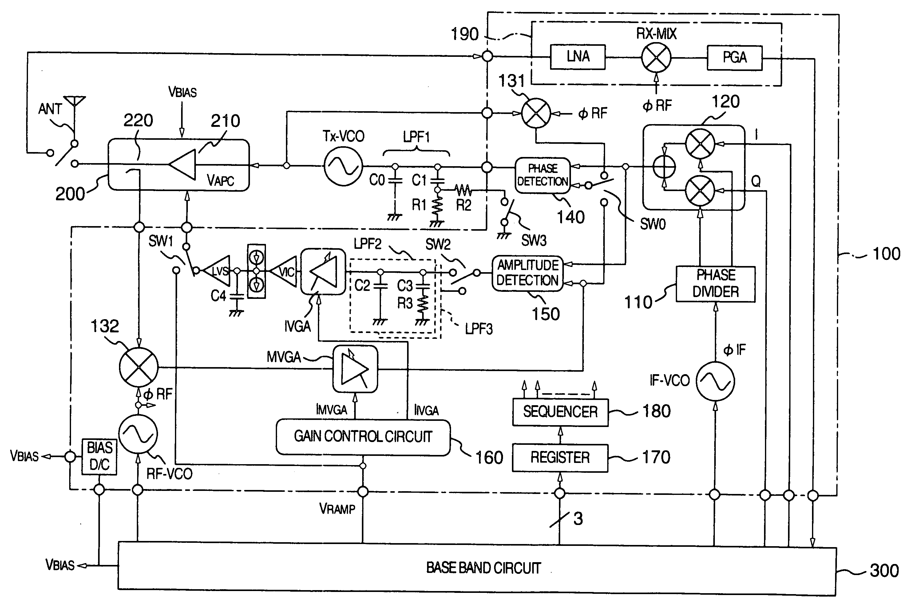
[0041]FIG. 1 shows a schematic configuration of a transmitter of a polar loop system according to an embodiment of the present invention. In FIG. 1, a reference numeral 100 represents a radio frequency IC which can perform GMSK modulation in a GSM system or 8-PSK modulation in an EDGE system; 200, a power module including a radio frequency power amplification circuit (hereinafter referred to as “power amplifier”) 210 for driving an antenna ANT so as to perform transmission, a coupler 220 for detecting transmitting power, and so on; 300, a base band circuit for generating I / Q signals on the basis of transmitting data (base band signal) or generating a control signal for the radio frequency IC 100 or a bias voltage VBIAS for the power amplifier 210 in the power module 200; TxVCO, a transmitting oscillator for generating a phase-modulated transmitting signal (carrier signal), and LPF1, a loop filter for limiting the bandwidth of a phase control loop.

[0042] The radio frequency IC 100 i...


PUM


Abstract

A transmitter adopting a polar loop system including a phase control loop for controlling the phase of a carrier signal outputted from a transmitting oscillator and an amplitude control loop for controlling the amplitude of a transmitting output signal outputted from a power amplification circuit, and designed to be capable of performing transmission using a GMSK modulation mode and transmission using an 8-PSK modulation mode. In the transmitter, the phase control loop is shared as a phase control loop for use in the GMSK modulation mode and a phase control loop for use in the 8-PSK modulation mode. A component similar to any one of components constituting a loop filter is provided in parallel therewith so that the component can be connected or disconnected in accordance with the modulation mode, for example, by use of a switching element.

Description

CROSS-REFERENCE TO RELATED APPLICATIONS [0001] The present application relates to subject matters described in the U.S. patent applications being file based on the United Kingdom Patent Applications No. 0212737.1 filed on May 31, 2002, No. 0212725.6 filed on May 31, 2002, No. 0212723.1 filed on May 31, 2002, No. 0212735.5 filed on May 31, 2002, and No. 0212732.2 filed on May 31, 2002. All of those U.S. applications are assigned to the same assignees of the present application. BACKGROUND OF THE INVENTION [0002] The present invention relates to a technique effective in application to a radio communication system having a phase control loop and an amplitude control loop for phase and amplitude modulation, and more particularly relates to a technique effective in application to a semiconductor integrated circuit for communication with a phase detection circuit and an amplitude detection circuit built in, and to a transmitter such as a cellular phone in which such a semiconductor integr...

Claims


Application Information

Patent Timeline
Patent Type & Authority Applications(United States)
IPC IPC(8): H04B1/02H04B1/66H04B1/04H04L27/12H04L27/00H04L27/20H04L27/36
CPCH03C5/00H04B1/0475H04B2001/0433H04L27/0008H04L27/2017H04L27/2071H04L27/361H03F1/34H03F3/24
Inventor TAKANO, RYOICHIHIKASA, KAZUHIKOKIMURA, YASUYUKIHAGISAWA, HIROSHIWURM, PATRICKHENSHAW, ROBERT ASTLEFREEBOROUGH, DAVID
Owner GOOGLE TECH HLDG LLC
Why Eureka
Try Eureka