Method and apparatus for selective deposition of materials to surfaces and substrates

a technology of material deposition and surface, applied in the direction of liquid/solution decomposition chemical coating, chemical vapor deposition coating, coating, etc., can solve the problems of insufficient deposition of materials, and inability to achieve efficient, optimal, and/or proper deposition of materials

Inactive Publication Date: 2006-10-05
BATTELLE MEMORIAL INST
View PDF8 Cites 31 Cited by
  • Summary
  • Abstract
  • Description
  • Claims
  • Application Information

AI Technical Summary

Benefits of technology

[0007] In another aspect, a system of the invention generally comprises a chamber for staging a substrate having a deposition surface; delivery means for delivering a solvent fluid and a precursor miscible in the solvent and optionally a chemical additive or reagent to the substrate at a liquid, near-critical, or supercritical temperature for the solvent; a heating source(s), the surface being disposed in an operable thermal relationship with the heating source(s) for generating a temperature gra

Problems solved by technology

As the footprint of critical feature patterns continues to decrease, efficient, optimum, and/or proper d

Method used


Image

  • Method and apparatus for selective deposition of materials to surfaces and substrates
  • Method and apparatus for selective deposition of materials to surfaces and substrates
  • Method and apparatus for selective deposition of materials to surfaces and substrates

Examples


example 1

[0057] Ruthenium is a promising electrode material in G-bit-scale dynamic random access memories (DRAMs) given its low resistivity, excellent chemical stability and good dry etching properties. In an example of the invention illustrated in FIG. 6, ruthenium metal was selectively deposited in vias 90 (pattern features) of a semiconductor chip substrate 42 filling vias 90. The system involves a solvent fluid 59 comprising densified carbon dioxide, a ruthenium metal precursor, Ru3(CO)12, stable at liquid, near-critical or supercritical temperatures for the solvent fluid, and a stoichiometric excess of a reagent gas, e.g., H2, preventing undesired oxidation reactions in the deposition vessel. Elemental ruthenium (Ru°) released from precursor 58 at or above the decomposition temperature for precursor 58 was deposited to substrate 42 selectively filling pattern vias 90. Substrate 42 was sized by scoring and breaking along the crystal planes, yielding a coupon of about 1 in. to 1.75 in. on...

example 2

[0060] In a further example of the invention illustrated in FIG. 8, copper metal was selectively deposited in the vias 90 (pattern features) of a semiconductor chip substrate 42 selectively filling the vias 90. The system comprises a solvent fluid 59 of densified carbon dioxide, a copper metal precursor 58, e.g., copper (II) hexafluoroacetylacetonate [Cu(hfac)2] (Sigma-Aldrich, Milwaukee, Wis.), and a stoichiometric excess of a reagent gas (H2). Copper (Cu+2) is released from precursor 58 to the deposition surface(s) of the vias 90 and reduced by the H2 reagent selectively filling the vias 90. Substrate 42 had dimensions of about 1 in. to 1.75 in. on a side. Vias 90 had a horizontal length dimension of 1 μm and a depth of ˜200 nm.

[0061] Experimental. 25 mg of solid precursor, e.g., Cu(hfac)2, was weighed into vessel 12 and placed underneath stage 38 in chamber 82. A semiconductor chip substrate 42 as described in Example 1 was secured to ceramic heating stage 38. Vessel 12 was seal...

example 3

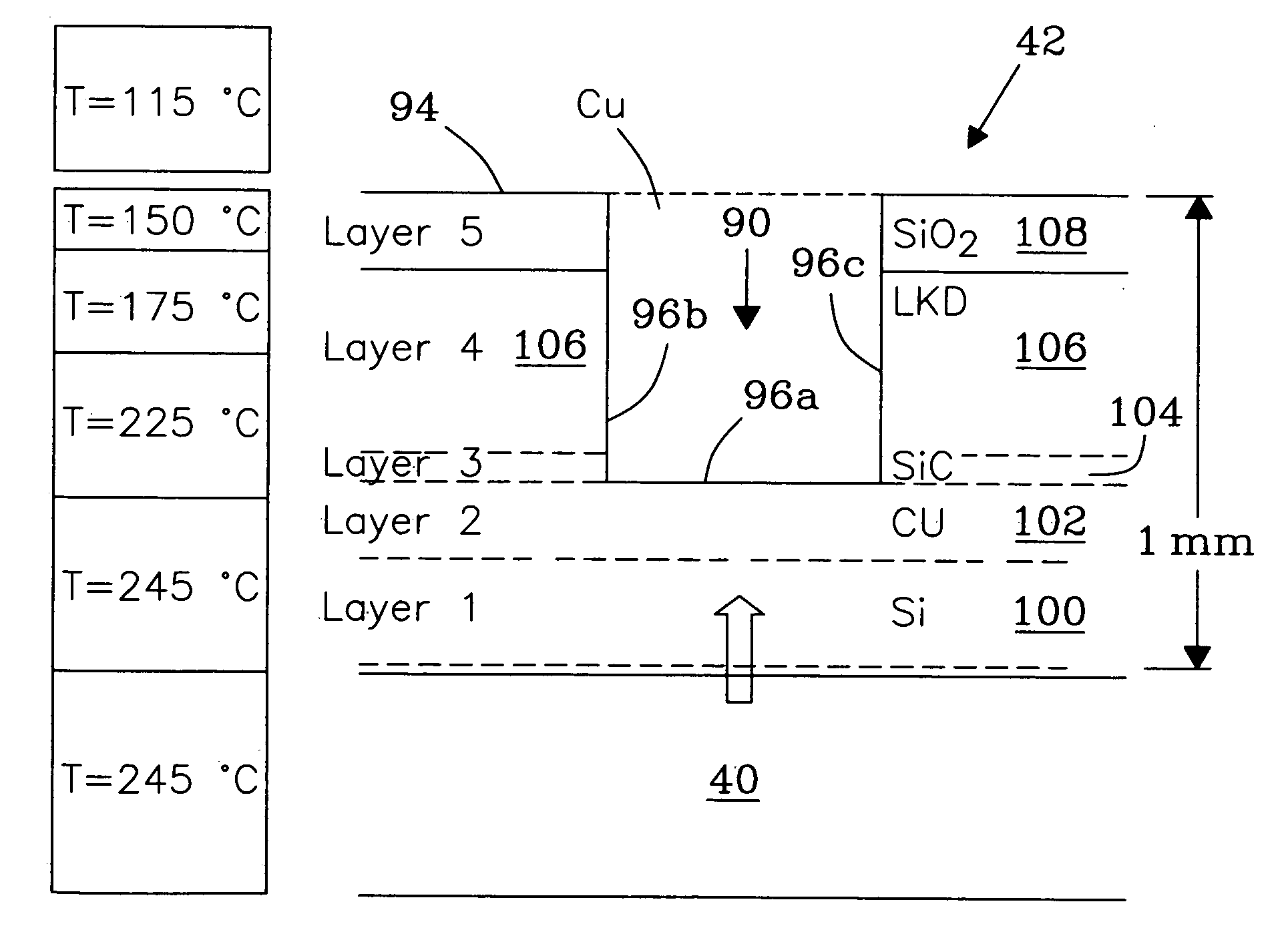
[0063] In another example of selective deposition illustrated in FIG. 9, ruthenium metal was selectively deposited in vias 90 of a semiconductor chip substrate 42 partially coating the vias 90 along a temperature gradient generated therein. A ruthenium metal precursor, Ru3(CO)12, and a stoichiometric excess of a reagent gas, e.g., H2, that prevents undesirable oxidation from miscellaneous oxygen sources in the reaction chamber during deposition, were mixed in a solvent fluid 59 of densified CO2. A temperature gradient was generated in the vias 90 in conjunction with a heating source 40 such that elemental ruthenium (Ru°) released from precursor 58 (e.g., above the release temperature for the precursor 58) was selectively deposited to surfaces within the vias 90 where temperature was above the release temperature for the precursor 58 thereby coating vias 90 along the temperature gradient. Substrate coupons 42 were sized by scoring and breaking along the crystal planes yielding a coup...


PUM

PropertyMeasurementUnit
Depthaaaaaaaaaa
Depthaaaaaaaaaa
Depthaaaaaaaaaa

Abstract

Methods are disclosed for depositing materials selectively and controllably from liquid, near-critical, and/or supercritical fluids to a substrate or surface controlling the location and/or thickness of material(s) deposited to the surface or substrate. In one exemplary process, metals are deposited selectively filling feature patterns (e.g., vias) of substrates. The process can be further used to control deposition of materials on sub-surfaces of composite or structured silicon wafers, e.g., for the deposition of barrier films on silicon wafer surfaces. Materials include, but are not limited to, overburden materials, metals, non-metals, layered materials, organics, polymers, and semiconductor materials. The instant invention finds application in such commercial processes as semiconductor chip manufacturing. In particular, selective deposition is envisioned to provide alternatives to, or decrease need for, such processes as Chemical Mechanical Planarization of silicon surfaces in semiconductor chip manufacturing due to selective filling and/or coating of pattern features with metals deposited from liquid, near-critical, or supercritical fluids.

Description

FIELD OF THE INVENTION [0001] The present invention relates generally to a method and an apparatus for selective deposition of materials. More particularly, the invention relates to a method and an apparatus for selectively depositing materials to a surface or substrate thereby controlling thickness of the material deposited at, on, in, and / or along the surface or substrate. The instant invention finds application in such commercial processes as semiconductor chip manufacturing. BACKGROUND OF THE INVENTION [0002] Semiconductor chips used in a multitude of electronic devices are structured or composite substrates fabricated from materials including semiconductors, dielectrics, metals, metal oxides, and patterned films comprising these materials. For example, the critical circuitry and interconnects on semiconductor chips require deposition of metals including, but not limited to, copper, aluminum, tungsten, tantalum, and ruthenium in pattern features, e.g., vias and trenches of the c...

Claims


Application Information

Patent Timeline
IPC IPC(8): H01L21/44C23C16/00
CPCC23C18/02C23C18/08H01L21/76879H01L21/76843H01L21/28562C23C16/04B82Y30/00C23C16/52C23C16/46H01L21/67207
Inventor YONKER, CLEMENT R.MATSON, DEAN W.GASPAR, DANIEL J.DEVERMAN, GEORGE S.
Owner BATTELLE MEMORIAL INST
Why Eureka
Try Eureka