Salicide process

a technology of sodium chloride and salt, applied in the direction of sodium chloride devices, basic electric elements, electrical equipment, etc., can solve the problems of deterioration of metal silicide sheet resistance, rough and non-uniform grains, etc., to achieve the reduction of metal suicide sheet resistance and junction leakage, avoid roughness of metal silicide grain, and improve metal silicide grain uniformity

Active Publication Date: 2006-10-19
MARLIN SEMICON LTD
View PDF7 Cites 1 Cited by
  • Summary
  • Abstract
  • Description
  • Claims
  • Application Information

AI Technical Summary

Benefits of technology

[0010] The second thermal process is conducted with two steps in which the first step is for nucleation while the second step is for grain growing so that the metal silicide grain roughness can be avoided and the metal suicide grain uniformity can be improved. Hence, metal suicide sheet resistance and junction leakage can be reduced.

Problems solved by technology

However, the metal suicide formed by the conventional two thermal processes causes rough and non-uniform grains because the metal silicide grains grow so rapidly that junction leakage is easily occurred and metal silicide sheet resistance is deteriorated.

Method used


Image

  • Salicide process
  • Salicide process
  • Salicide process

Examples


Embodiment Construction

[0015] Reference will now be made in detail to the present preferred embodiments of the invention, examples of which are illustrated in the accompanying drawing.

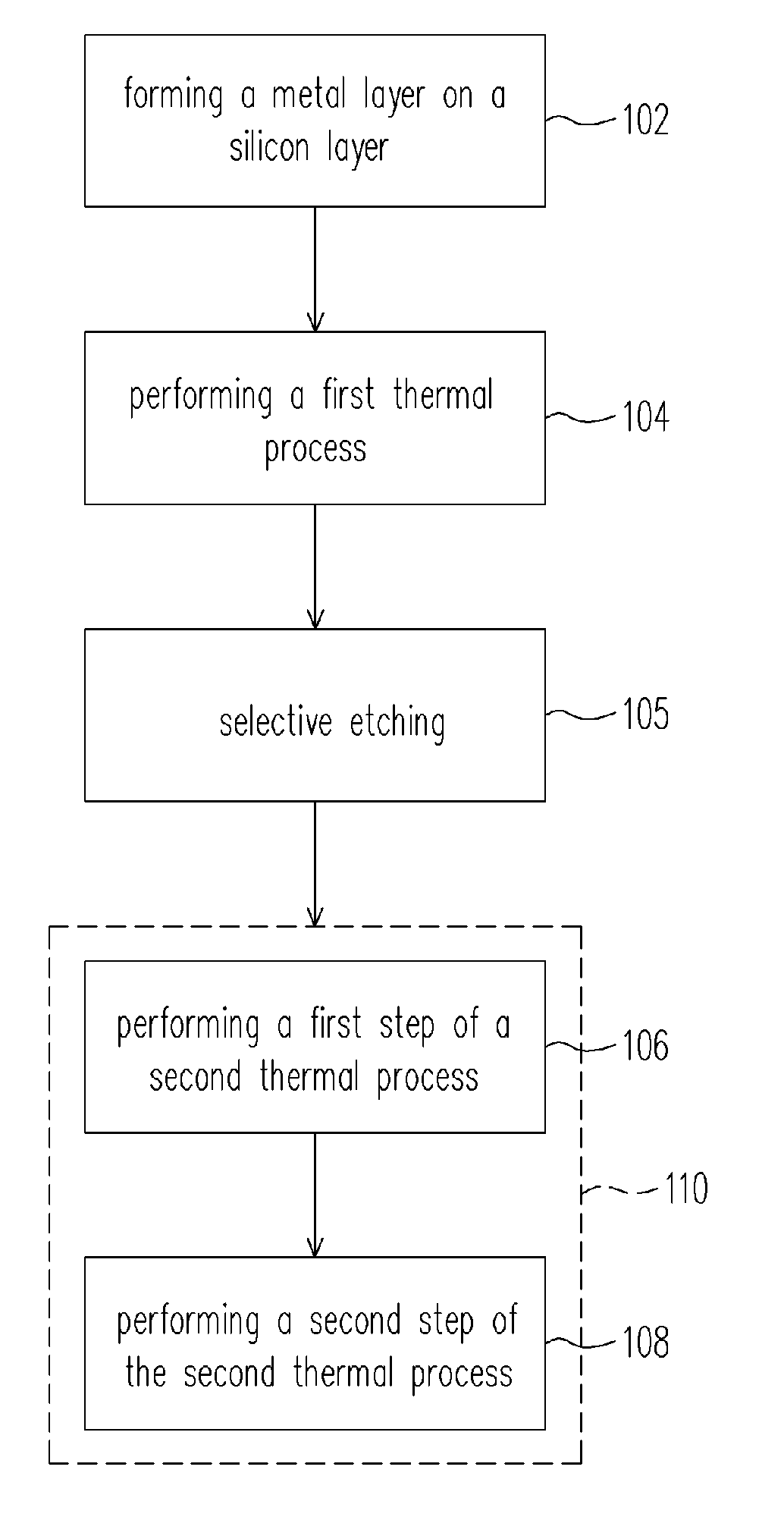
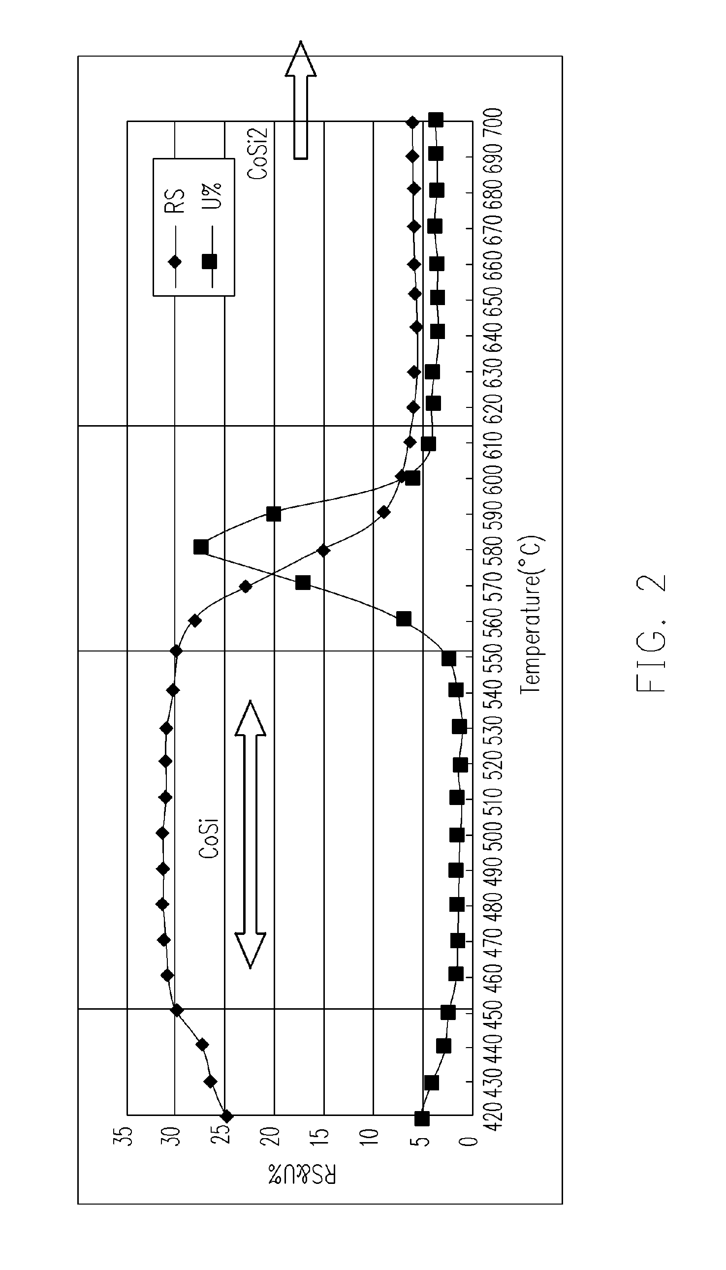
[0016]FIG. 1 is a flow chart showing a salicide process according to an embodiment of the present invention. As shown in FIG. 1, the salicide process of the present invention comprises the following steps, 102˜108. First, a metal layer is formed over a silicon layer (step 102). In an embodiment, the metal layer is selected from titanium, cobalt, platinum, palladium and an alloy thereof, for example. In another embodiment, the metal layer is selected from nickel and an alloy thereof, for example. The metal layer is formed with a sputtering deposition process, an evaporation process or other suitable deposition process. The silicon layer may be a silicon substrate, a polysilicon layer and the like. In an embodiment, the silicon layer comprises a source region, a drain region and a gate electrode of a MOS transistor, for examp...


PUM

PropertyMeasurementUnit
temperatureaaaaaaaaaa
feature sizeaaaaaaaaaa

Abstract

A salicide process is provided. A metal layer selected from a group consisting of titanium, cobalt, platinum, palladium and an alloy thereof is formed over a silicon layer. A first thermal process is performed. Next, a second thermal process is performed, wherein the second thermal process includes a first step performed at 600˜700 degrees centigrade for 10˜60 seconds and a second step performed at 750˜850 degrees centigrade for 10˜60 seconds. If the metal layer is selected from a group consisting of nickel and an alloy thereof is formed on a silicon layer, the first step of the second thermal process is performed at 300˜400 degrees centigrade for 10˜60 seconds and the second step of the second thermal process is performed at 450˜550 degrees centigrade for 10˜60 seconds.

Description

BACKGROUND OF THE INVENTION [0001] 1. Field of the Invention [0002] The present invention generally relates to a semiconductor process. More particularly, the present invention relates to a salicide process. [0003] 2. Description of Related Art [0004] Semiconductor device improvements have been largely accomplished by reducing device feature size while predictions for future device sizes do not foresee an end to the trend of ever smaller and denser devices. Reduction in MOS transistor device feature size brings with it reduction in film thickness while the depth of diffusion regions is also reduced. For the salicide process that is used to establish electrical contacts with the active regions, a metal layer is formed over these active regions (the source / drain region and the gate electrode) and subjected to a thermal process. [0005] For several salicide processes, such as titanium and cobalt salicide processes, two thermal processes for annealing are conducted because these metal su...

Claims


Application Information

Patent Timeline
Patent Type & Authority Applications(United States)
IPC IPC(8): H01L21/28
CPCH01L29/665H01L21/28518
Inventor CHEN, MIN-HSIANHSIEH, CHING-HSING
Owner MARLIN SEMICON LTD
Why Eureka
Try Eureka