Semiconductor package structure and method for separating package of wafer level package

a technology of semiconductor devices and package structures, applied in semiconductor devices, semiconductor/solid-state device details, electrical equipment, etc., can solve the problems of affecting the cutting quality of the saw blad

Inactive Publication Date: 2007-06-07
ADVANCED CHIP ENG TECH
View PDF4 Cites 15 Cited by
  • Summary
  • Abstract
  • Description
  • Claims
  • Application Information

AI Technical Summary

Benefits of technology

[0014] The dicing method of semiconductor device package of the present invention can avoid the roughness on the edge of each package after dicing with a dicing saw.
[0015] The dicing method of the present invention may avoid the high cost owing to using a dicing saw.
[0016] The dicing method of the present invention may reduce cycle time throughout the dicing process.
[0021] The above-mentioned buffer layer may reach the function to avoid the die or substrate from damaging when the side part of the die or substrate collides with an external object.

Problems solved by technology

While saw cutting of wafers and panel is the conventional industry standard, there remain drawbacks with such cutting.
Saw blade wear over time.
This results in inconsistent cutting quality from when the blade is new and subsequent cutting operations.
This cannot be predicted accurately.
Accordingly, the saw blades may be changed before the end of their useful lives resulting in higher equipment costs than necessary due to premature saw blade replacement.
Moreover, saw blades introduce mechanical stresses in the workpiece while sawing, especially at the surfaces of the workpiece.
Due to these stresses saw blade may not be used to cut very thin workpiece, such as ultrathin semiconductor wafers.
Increasing use of integrated circuits (IC's) technology in microwave and hybrid circuits, memories, computers, defense and medical electronics has created new difficult problems for the industry.
The other drawback of using saw is time consuming.
It affects not only the throughput of products, but the cost of processing a wafer and panel.
The cost of the method of dicing wafer using the saw blade is higher due to the blades are not ordinary blades, they are more expensive than general knifes.
There is still a drawback by a dicing saw with a saw blade.

Method used


Image

  • Semiconductor package structure and method for separating package of wafer level package
  • Semiconductor package structure and method for separating package of wafer level package
  • Semiconductor package structure and method for separating package of wafer level package

Examples


Embodiment Construction

[0027] Method and structure for manufacturing a semiconductor device (such as integrated circuit) or a substrate is described below. In the following description, numerous specific details are set forth in order to provide a thorough understanding of the present invention, and the scope of the present invention is expressly not limited expect as specified in the accompanying claims.

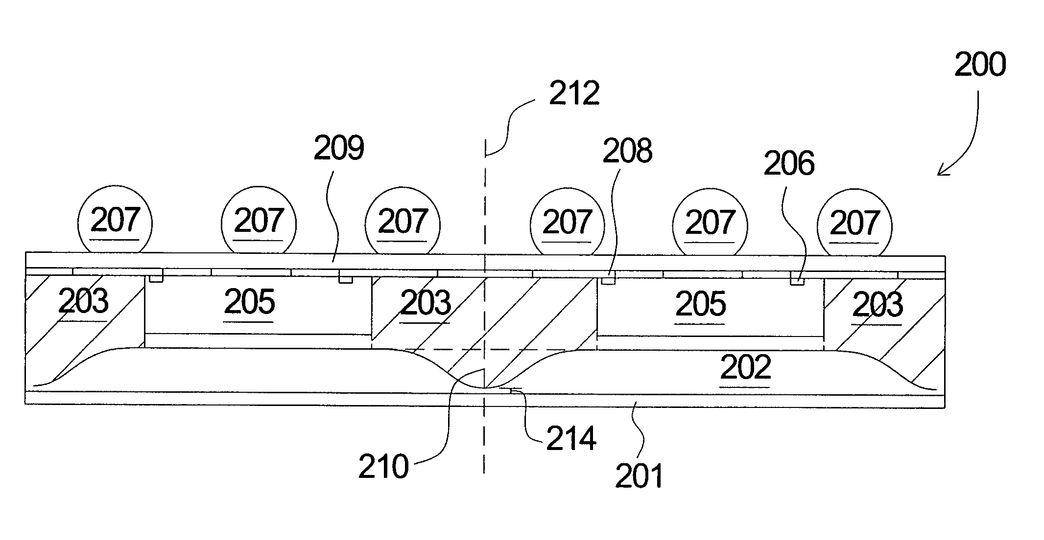
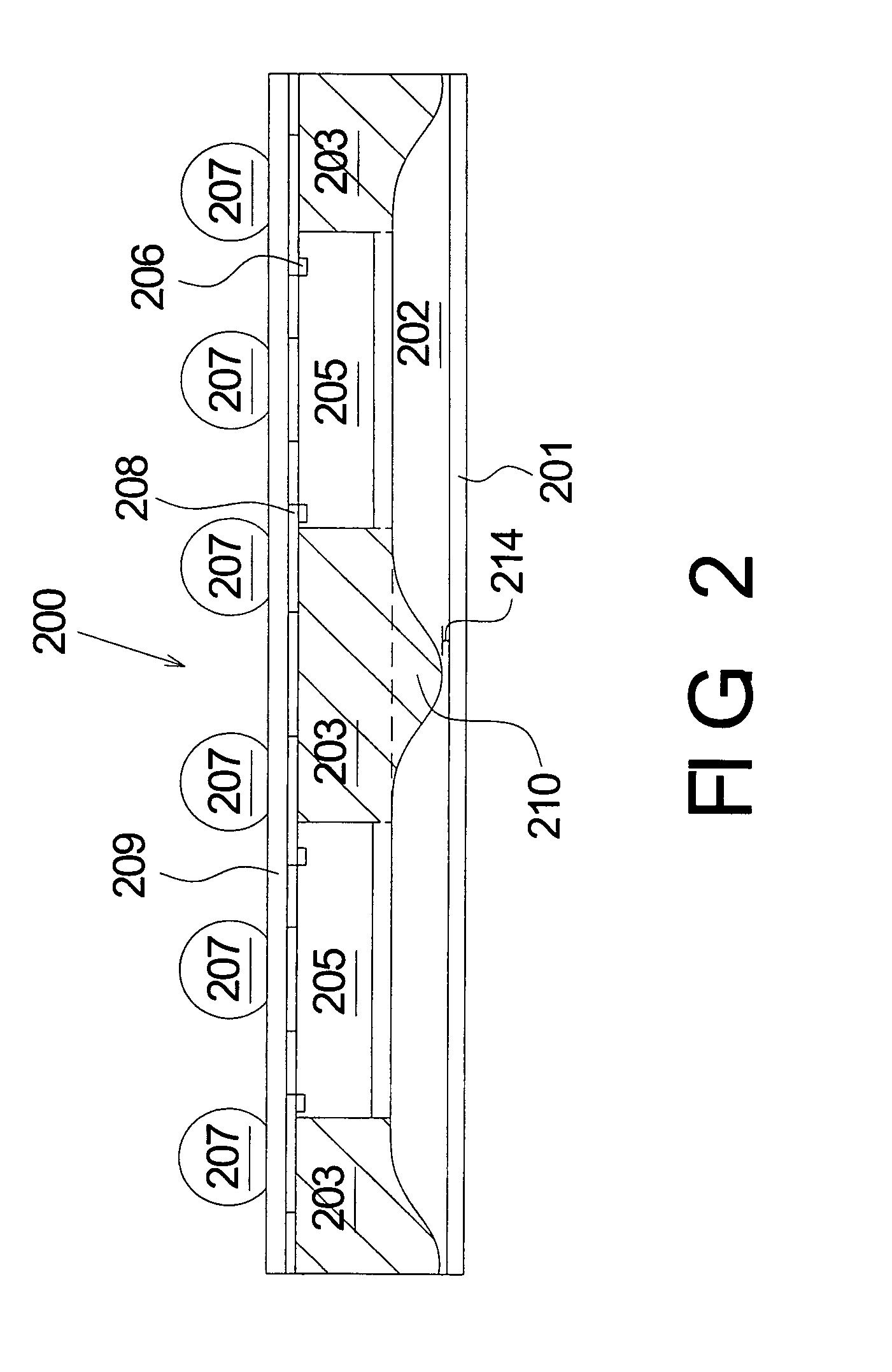
[0028] Referring to FIG. 2, the wafer 200 comprises plurality of chip 205 with metal pads 206 and contact metal balls 207 formed thereon and electrically coupled with a print circuit board (not shown). A protection layer 209 covers the electrical connections 208 to expose a portion of the electrical connections 208 for allowing the contact metal balls 207 formed thereon.

[0029] A backside surface of the chip 205 is directly adhered on a substrate 202 with recesses substantially aligned to a first buffer layer 203. The recesses may be formed by using a wet etching process prior to the adhesion to the wafe...


PUM


Abstract

The present invention provides a separating process of a semiconductor device package of wafer level package. The method comprises a step of etching a substrate to form recesses. Then a buffer layer is formed on the first surface of the substrate, wherein the buffer layer is filled with the corresponding recesses to form infillings on adjacent the semiconductor device package. Dicing the wafer into individual package along substantial center of said infillings, the step may avoid the roughness on the edge of each die and also decrease the cost of the separating process.

Description

BACKGROUND OF THE INVENTION [0001] 1. Field of the Invention [0002] This invention relates generally to semiconductor device packaging, and more particularly to a dicing method of semiconductor devices package for dividing a wafer or panel into discrete package. [0003] 2. Description of the Prior Art [0004] In the electronic component world, integrated circuits (IC's) are typically fabricated on a semiconductor substrate, known as a chip, and most commonly are made of silicon. The silicon chip is typically assembled into a larger package, which serves to provide effective enlargement of the distance or pitch between input / output contacts of the silicon making it suitable for attachment to a printed circuit board, and to protect the IC from mechanical and environmental damage. [0005] Conventionally, ICs are packaged one by one after dicing from a wafer. A wafer level package (WLP) or a chip scale package (CSP) was developed to provide an alternative solution to directly attached flip...

Claims


Application Information

Patent Timeline
Patent Type & Authority Applications(United States)
IPC IPC(8): H01L21/00H01L21/4763
CPCH01L21/561H01L23/13H01L23/16H01L23/3128H01L24/97H01L2224/97H01L2924/01029H01L2924/01079H01L2924/01094H01L2924/09701H01L2224/19H01L2924/01005H01L2924/01006H01L2924/01033H01L2924/10253H01L2924/00H01L2924/15787H01L2924/14H01L2224/12105H01L2224/73267H01L2224/83
Inventor YANG, WEN-KUNCHANG, JUI-HSIEN
Owner ADVANCED CHIP ENG TECH
Why Eureka
Try Eureka