Method of manufacturing semiconductor device having shallow junction

a semiconductor device and manufacturing method technology, applied in the direction of semiconductor devices, basic electric elements, electrical appliances, etc., can solve the problems of difficult to sufficiently shallowly diffuse ions, unnecessary impurities, damage to the front surface of silicon substrates,

Inactive Publication Date: 2001-04-17
RENESAS ELECTRONICS CORP
View PDF1 Cites 17 Cited by
  • Summary
  • Abstract
  • Description
  • Claims
  • Application Information

AI Technical Summary

Problems solved by technology

However, in such known methods, unnecessary impurities other than desired impurities would be doped to the substrate.
In addition, when the ion doping process and the annealing process are performed, the front surface of the silicon substrate may be damaged.
However, it is difficult to sufficiently shallowly diffuse ions in the method of which ions are doped through the through-oxide film.
When ions are doped to a silicon substrate, point defects take place in the silicon substrate.

Method used


Image

  • Method of manufacturing semiconductor device having shallow junction
  • Method of manufacturing semiconductor device having shallow junction
  • Method of manufacturing semiconductor device having shallow junction

Examples


Embodiment Construction

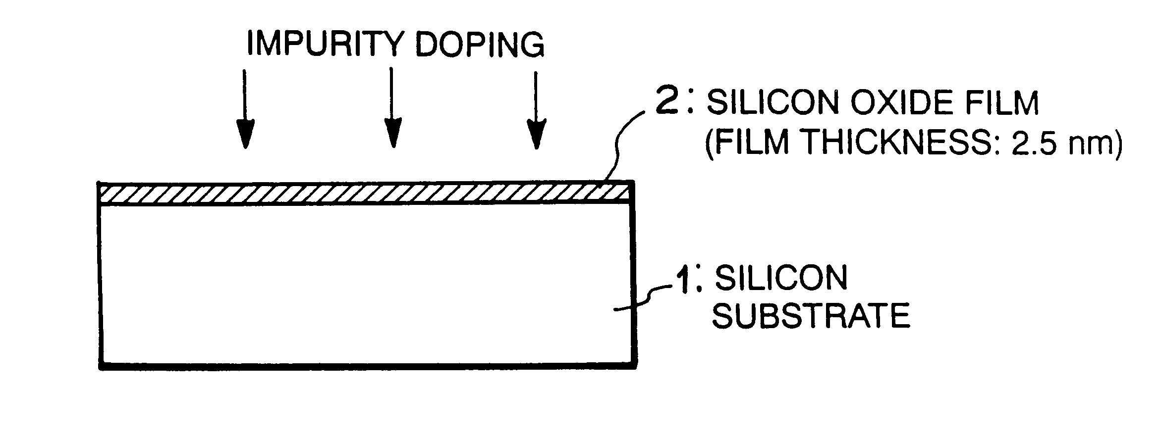
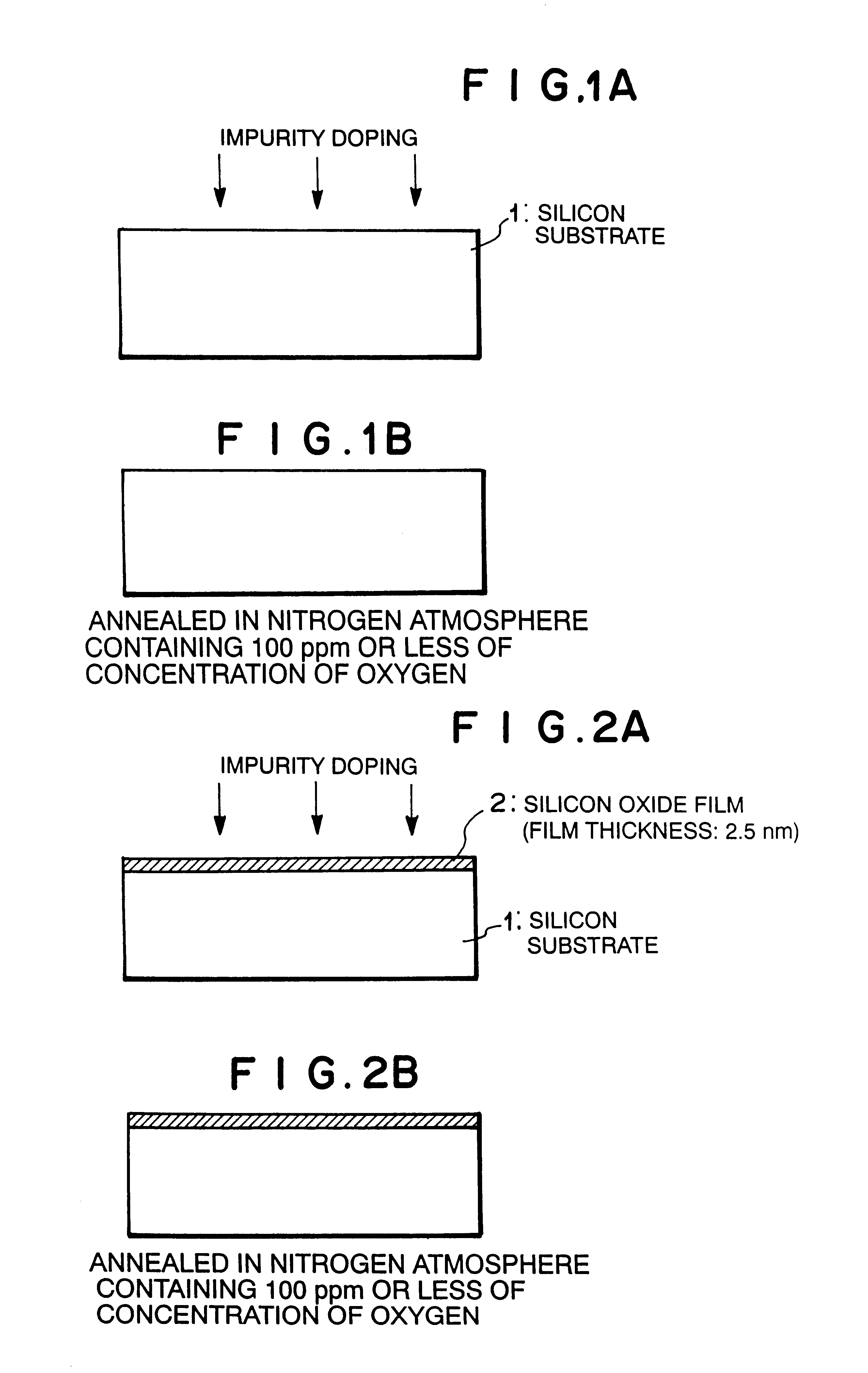
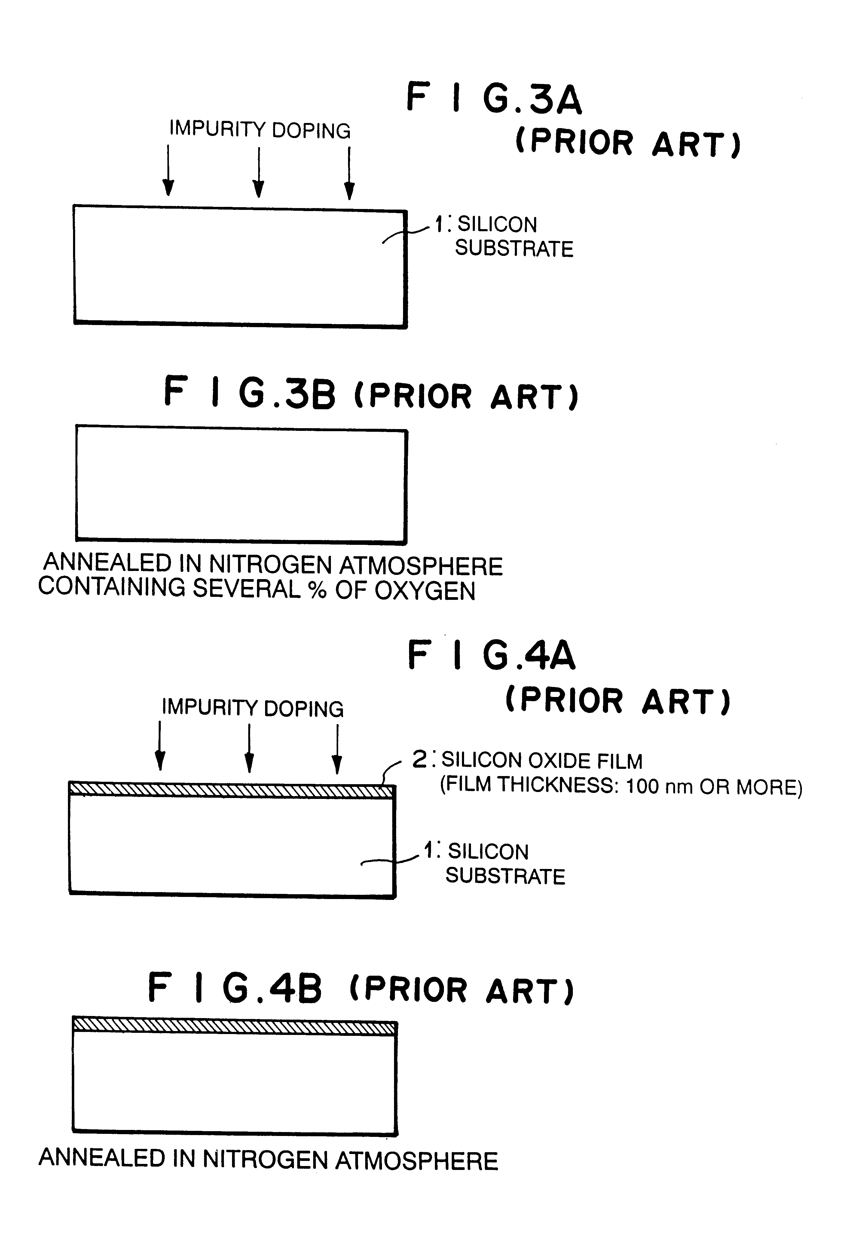
Next, with reference to the accompanying drawings, embodiments of the present invention will be described. FIGS. 1A and 1B are schematic diagrams showing an example of a method of manufacturing a semiconductor device according to the present invention. In the method, ions of impurities are doped to the front surface of a wafer without a through-oxide film. The ions are doped at an accelerating voltage of 3 keV or less. At such an accelerating voltage, shallow junctions are preferably formed. Thus, in the ion doping process, the front surface thereof can be sufficiently suppressed from roughening. The impurities considered in the present invention are boron, boron fluoride, phosphorus, arsenic, antimony, or the like that are conventionally used for doping carriers. According to the present invention, the concentration of doped ions is not limited. In other words, the concentration can be properly set.

After ions of impurities are doped to a substrate, the impurities are heat-diffused ...


PUM

PropertyMeasurementUnit
thicknessaaaaaaaaaa
temperatureaaaaaaaaaa
thicknessaaaaaaaaaa

Abstract

A method of manufacturing a semiconductor device having a silicon substrate containing an impurity diffusion layer is disclosed, that comprises the steps of doping impurities to the silicon substrate through a silicon oxide film with a thickness of 2.5 nm or less at an accelerating voltage of 3 keV or less, the silicon oxide film being formed on the silicon substrate and annealing the silicon substrate with the oxide film left.

Description

1. Field of the InventionThe present invention relates to a method of manufacturing a semiconductor device having an impurity diffusion layer, in particular, to a method of manufacturing a semiconductor device having shallow junctions.2. Description of the Related ArtFIG. 3A and FIG. 3B show an example of prior art ion doping technologies. In this method, ions are directly doped to a substrate with an accelerating voltage of 5 to 80 keV. Thereafter, the substrate is annealed in a nitrogen atmosphere containing oxygen in the state that the front surface thereof is exposed so as to form a diffusion layer.However, in such known methods, unnecessary impurities other than desired impurities would be doped to the substrate. In addition, when the ion doping process and the annealing process are performed, the front surface of the silicon substrate may be damaged.To solve such a problem, a silicon oxide film is formed on the substrate. Ions are doped through the silicon oxide film (hereinaf...

Claims


Application Information

Patent Timeline
Patent Type & Authority Patents(United States)
IPC IPC(8): H01L21/02H01L21/265H01L21/324H01L21/316
CPCH01L21/2652H01L21/324H01L21/31662Y10S438/92H01L21/02164H01L21/22
Inventor YASUNAGA, TOMOKO
Owner RENESAS ELECTRONICS CORP
Why Eureka
Try Eureka