Selective deposition of silicon-containing films

a technology of silicon-containing films and selective deposition, which is applied in the direction of polycrystalline material growth, crystal growth process, chemically reactive gas, etc., can solve the problems of few advantages, few studies performed, and the development of commercial sources of trisilane not yet recognized, so as to improve the surface the quality of the deposited layer. the effect of high quality

Active Publication Date: 2006-10-19
ASM IP HLDG BV
View PDF99 Cites 144 Cited by
  • Summary
  • Abstract
  • Description
  • Claims
  • Application Information

AI Technical Summary

Benefits of technology

[0011] Deposition processes have now been discovered that are faster and result in higher quality deposited layers. Certain described processes employ trisilane (H3SiSiH2SiH3) as a silicon source and a halogen-containing etchant gas such as chlorine gas (Cl2) as a source of chlorine for providing selectivity to the deposition process of Si-containing films. Advantageously, the process works well with additive process gases, including carbon or germanium sources, for incorporation of strain into the deposited layer or adjacent structures, and / or dopant sources. For example, it has been found that selectively deposited crystalline silicon may be doped to contain relatively high levels of other elements (such as carbon, germanium and various electrically active dopants such as arsenic and phosphorous) by carrying out the deposition of the crystalline silicon using chlorine, trisilane (as a silicon source) and an additive process gas (such as a carbon source, germanium source and / or electrically active dopant precursor). Electrically active dopant precursors have been found to not only provide the desired conductivity in situ, obviating subsequent doping steps, but have also been found to independently improve surface quality of the deposited layer. Particular advantages have been found for use of non-hydrogen carrier gases in conjunction with trisilane / chlorine deposition recipes.

Problems solved by technology

While trisilane has been long been known as a theoretical precursor for silicon, few studies have been performed on it and few advantages have been recognized.
Accordingly, significant commercial sources of trisilane have not developed historically.

Method used


Image

  • Selective deposition of silicon-containing films
  • Selective deposition of silicon-containing films
  • Selective deposition of silicon-containing films

Examples


example 1

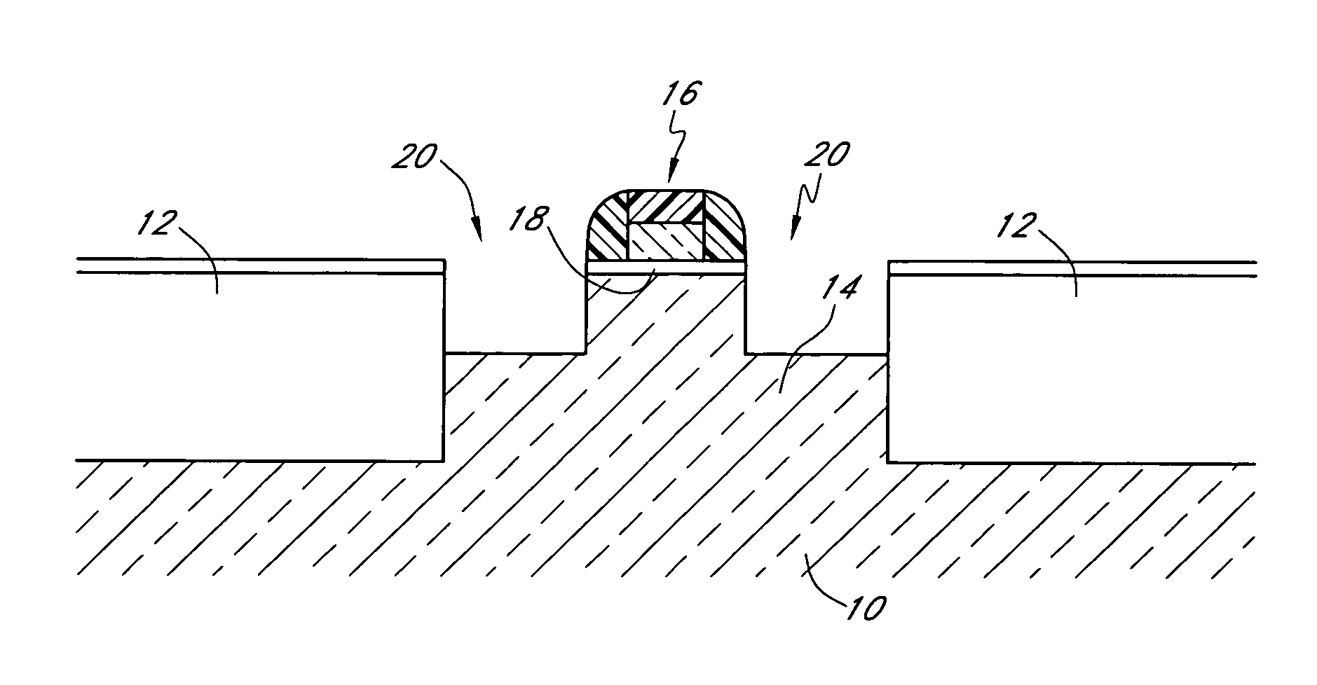
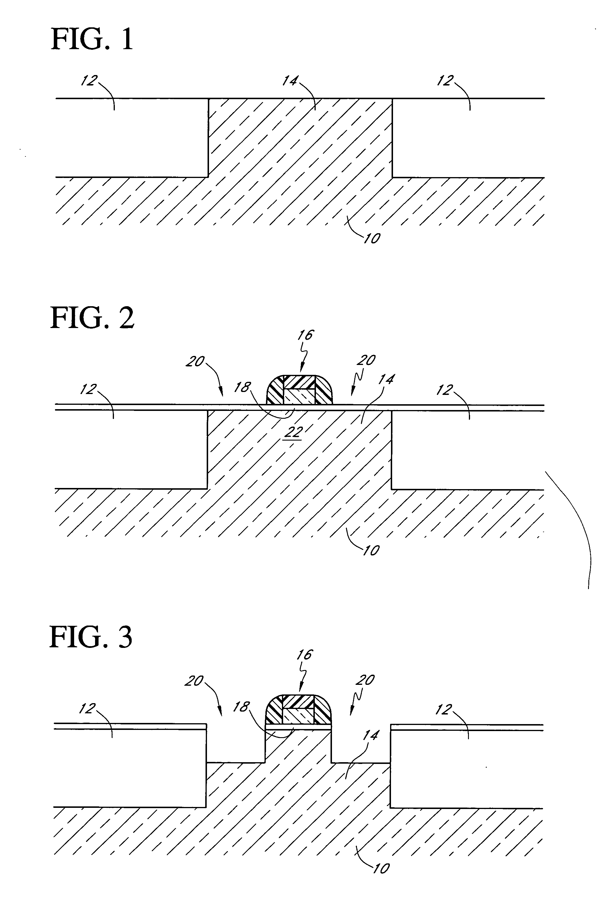
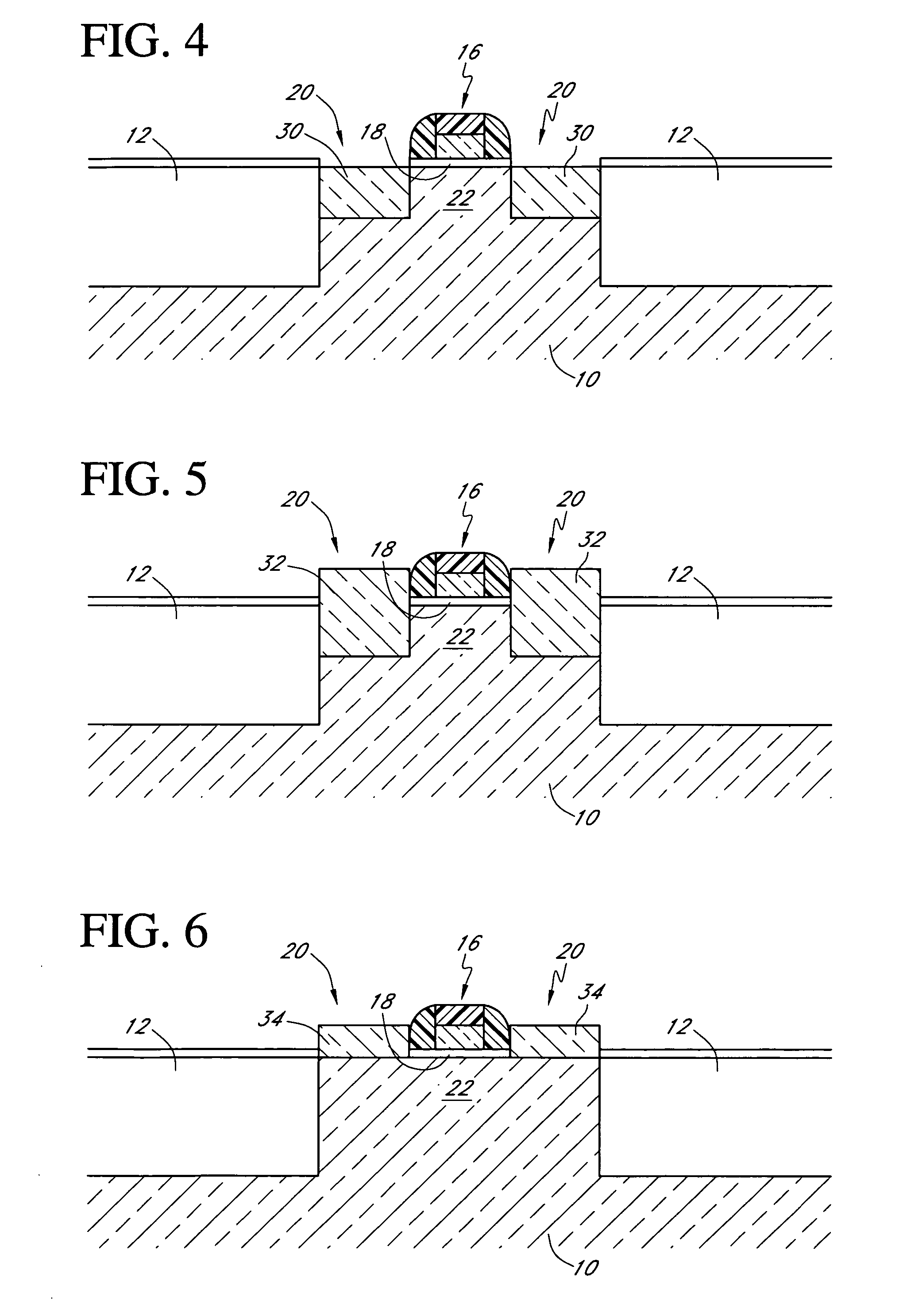
[0153] This example illustrates the selective deposition of epitaxial silicon films over mixed morphology substrates.

[0154] An eight-inch unpatterned Si wafer substrate and separate wafer with a fully oxidized (1000 Å) surface were loaded into an Epsilon E2500™ reactor system. The substrate was then introduced into the reactor system at 900° C., at a hydrogen flow rate of 20 slm, and the substrate was allowed to stabilize for 1 minute. The hydrogen flow was then shut down as the temperature of the substrate was reduced to 550° C. The substrate was then allowed to stabilize for 10 seconds, after which time a flow of 50 mg / min of trisilane was introduced for 10 minutes. A flow of 200 sccm chlorine gas and 100 sccm of 1% phosphine was simultaneously provided and the deposition was conducted at a deposition pressure of about 6 Torr. A continuous, uniform phosphorous-doped Si film having a thickness of about 500 Å was selectively deposited (deposition rate of 5 nm / min) over the single c...

example 2

[0155] A deposition process was conducted as described in Example 1 except that a separate wafer having a silicon nitride surface was loaded into the reactor system instead of the separate wafer with a silicon oxide surface. An epitaxial phosphorous-doped Si film was selectively deposited on the silicon wafer, with essentially no deposition on the silicon nitride surface. As in Example 1, the deposited phosphorous-doped Si film had excellent epitaxial quality and a resistivity of about 0.35 mΩ·cm.


PUM

PropertyMeasurementUnit
temperatureaaaaaaaaaa
pressureaaaaaaaaaa

Abstract

Chemical vapor deposition methods use trisilane and a halogen-containing etchant source (such as chlorine) to selectively deposit Si-containing films over selected regions of mixed substrates. Dopant sources may be intermixed with the trisilane and the etchant source to selectively deposit doped Si-containing films. The selective deposition methods are useful in a variety of applications, such as semiconductor manufacturing.

Description

CROSS-REFERENCE TO RELATED APPLICATIONS [0001] This application claims priority to U.S. Provisional Application No. 60 / 649,990, filed Feb. 4, 2005; U.S. Provisional Application No. 60 / 663,434, filed Mar. 18, 2005; and U.S. Provisional Application No. 60 / 668,420, filed Apr. 4, 2005; all of which are hereby incorporated by reference in their entireties. [0002] This application is related to, and incorporates by reference in their entireties, the following U.S. patent applications: U.S. patent application Ser. No. ______, entitled “METHODS OF MAKING SUBSTITUTIONALLY CARBON-DOPED CRYSTALLINE SI-CONTAINING MATERIALS BY CHEMICAL VAPOR DEPOSITION (ATTORNEY DOCKET NO. ASMEX.511A); and U.S. patent application Ser. No. ______, entitled “METHODS OF MAKING ELECTRICALLY DOPED CRYSTALLINE SI-CONTAINING FILMS (ATTORNEY DOCKET NO. ASMEX.527A), both of which are filed on even date herewith.BACKGROUND OF THE INVENTION [0003] 1. Field of the Invention [0004] This application relates generally to the d...

Claims


Application Information

Patent Timeline
Patent Type & Authority Applications(United States)
IPC IPC(8): H01L21/44
CPCC23C16/04H01L29/7848C23C16/24C23C16/32C23C16/325C23C16/45512C30B25/02C30B29/06H01L21/02381H01L21/02529H01L21/02532H01L21/02576H01L21/02579H01L21/0262H01L21/02636H01L21/02639H01L21/32056H01L21/3215H01L29/165H01L29/66628H01L29/66636H01L29/7834C23C16/22H01L29/10
Inventor BAUER, MATTHIASARENA, CHANTALBERTRAM, RONALDTOMASINI, PIERRECODY, NYLESBRABANT, PAULITALIANO, JOSEPHJACOBSON, PAULWEEKS, KEITH DORAN
Owner ASM IP HLDG BV
Why Eureka
Try Eureka