

OLED multicolor displays
- Summary
- Abstract
- Description
- Claims
- Application Information
AI Technical Summary
Benefits of technology
Problems solved by technology
Method used
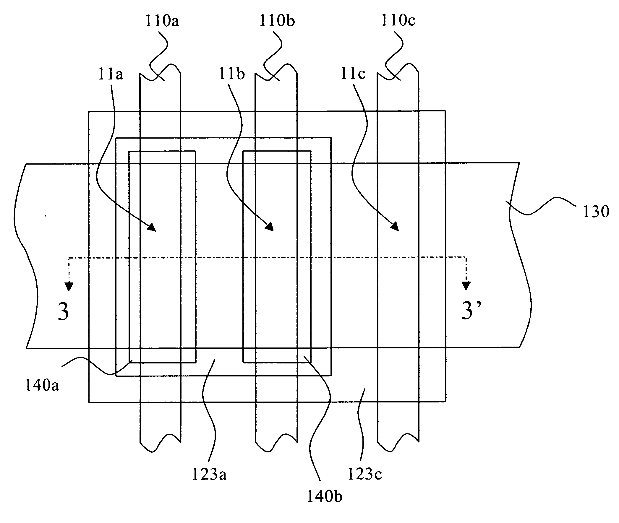
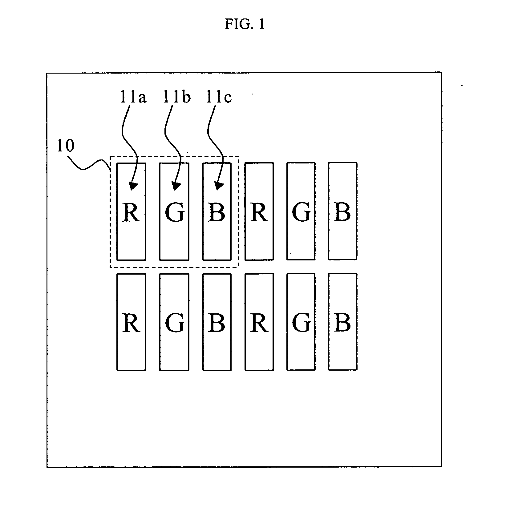
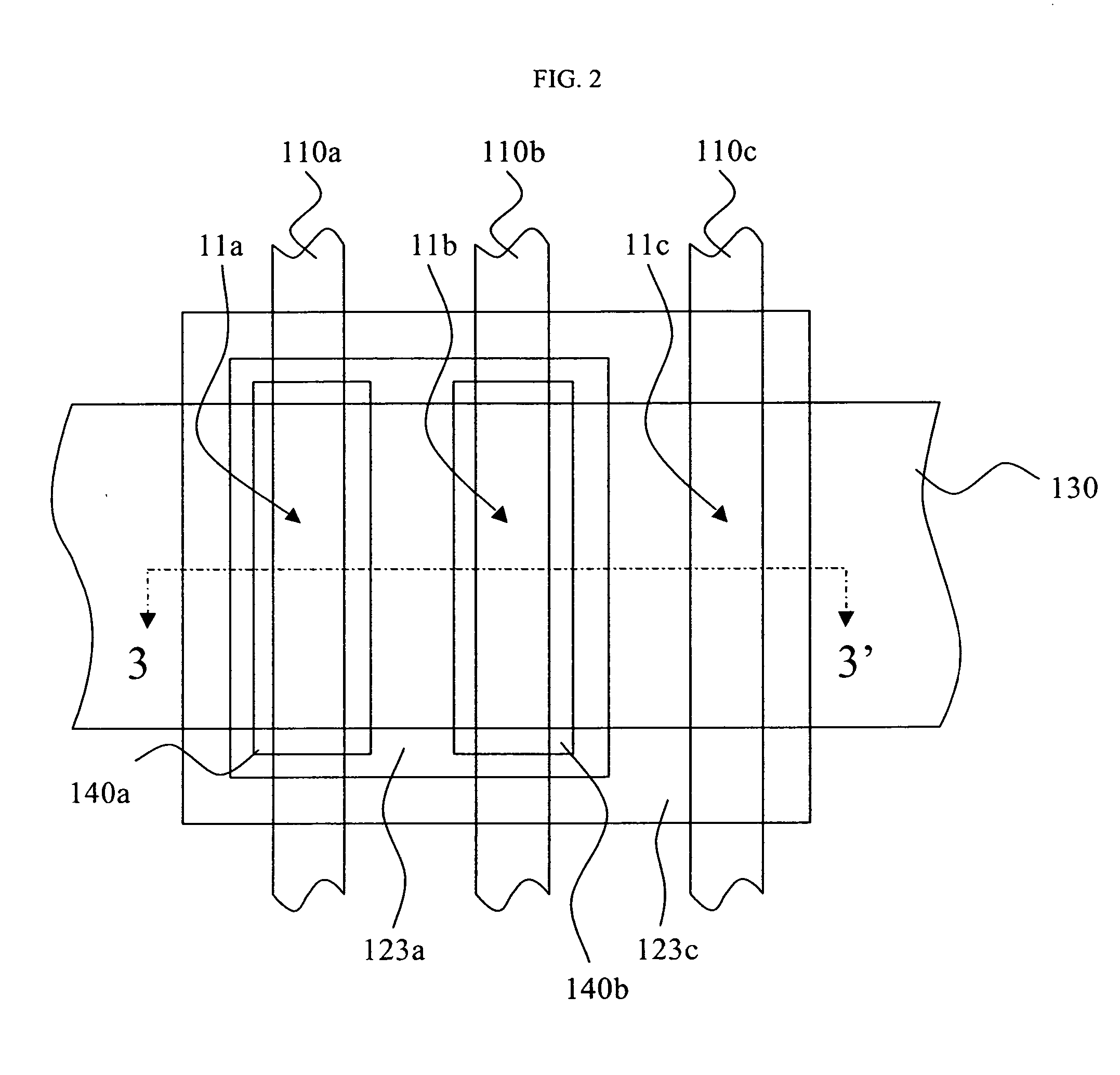
Image

Examples
example 1
Comparative
[0208] A comparative OLED device was constructed in the following manner:
[0209] 1. A clean glass substrate was vacuum-deposited with indium tin oxide (ITO) to form a transparent electrode of 85 nm thickness;
[0210] 2. The above-prepared ITO surface was treated with a plasma oxygen etch, followed by plasma deposition of a 0.5 nm layer of a fluorocarbon polymer (CFx) as described in U.S. Pat. No. 6,208,075;
[0211] 3. The above-prepared substrate was further treated by vacuum-depositing a 240 nm layer of 4,4′-bis[N-(1-naphthyl)-N-phenylamino]biphenyl (NPB) as a hole-transporting layer (HTL);
[0212] 4. A coating of 30 nm thickness, composed of 97.5% NPB (as host) with 2.5% yellow-orange emitting dopant 5,11-bis(biphenyl-4-yl)-6,12-bis(4-tert-butylphenyl)-3,9-di-tert-butylnaphthacene (Formula L50) were co-evaporatively deposited onto the HTL layer to form a yellow-orange emitting first light emitting layer;
[0213] 5. A coating of 45 nm thickness, composed of 92% 9-(2-naphthy...
example 2
[0217] Example 2 was prepared similar to Example 1, with the exception of the yellow-orange emitting layer, which included tBuDPN co-dopant (Formula P6). The yellow-orange emitting layer of Example 2 was composed of 78% NPB (as host) with 19.5% tBuDPN (Formula P6) and 2.5% of 5,11-bis(biphenyl-4-yl)-6,12-bis(4-tert-butylphenyl)-3,9-di-tert-butylnaphthacene (Formula L50). The blue layer, ETL and cathode layers were the same. The device was then transferred to a dry box for encapsulation.
example 3
[0218] Example 3 was prepared similar to Example 1, with the exception that the yellow-orange light emitting layer was not included, and the HTL layer was slightly thicker. The blue layer, ETL and cathode layers were the same. The device was then transferred to a dry box for encapsulation.
PUM
 Abstract
Description
Claims
Application Information