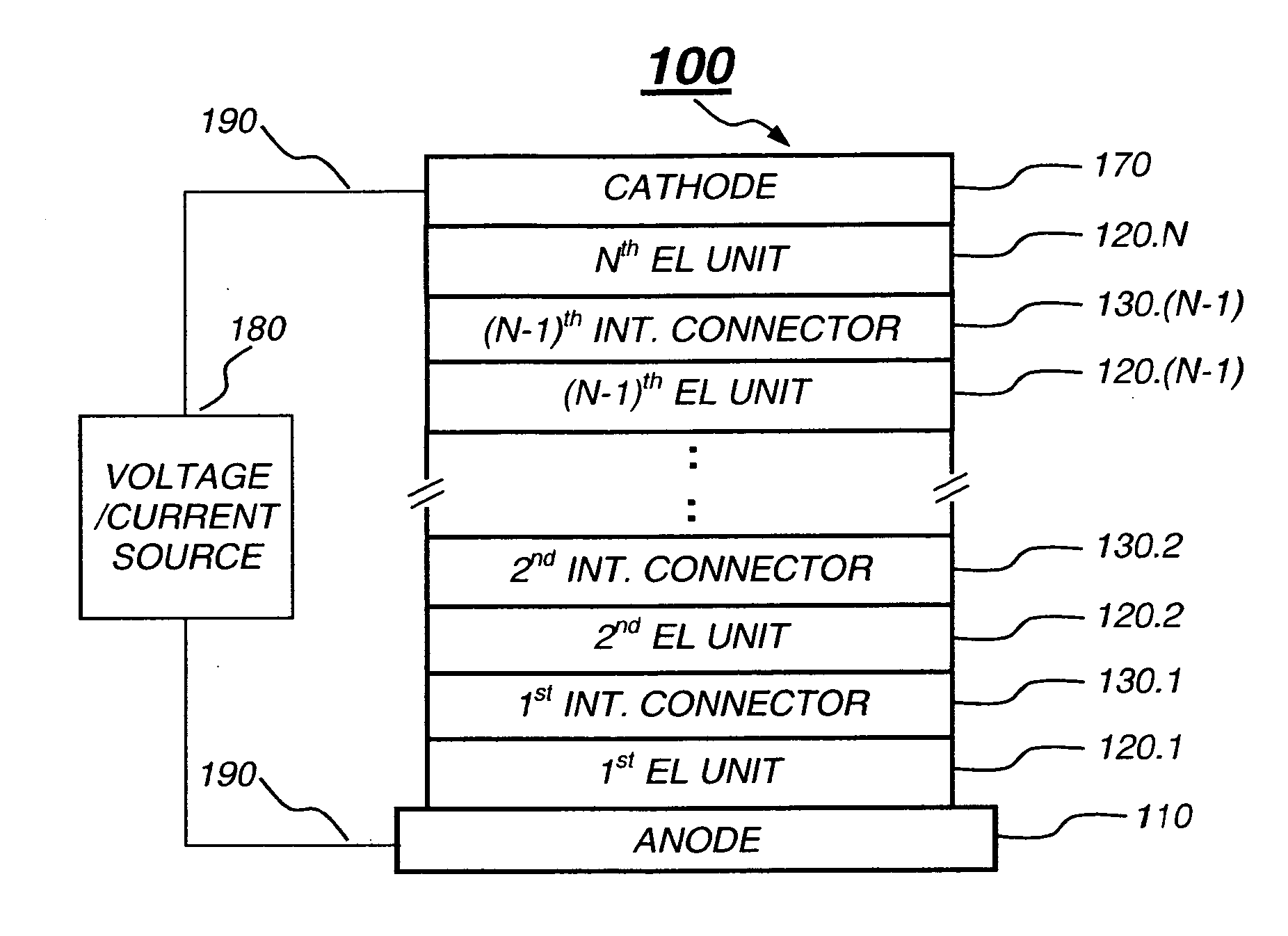
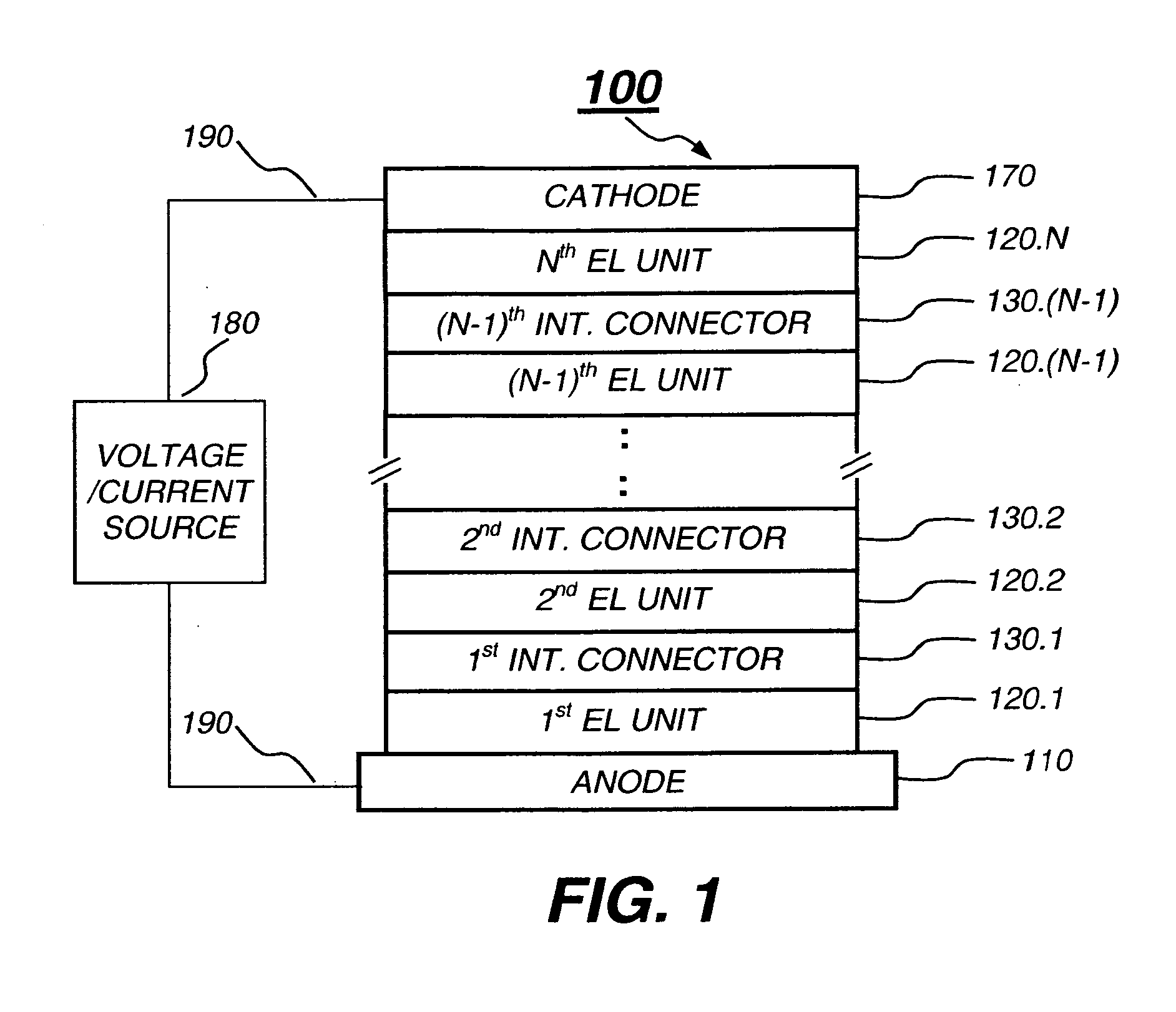
Tandem OLED device

a technology of oled device and oled ring, which is applied in the direction of organic semiconductor device, discharge tube luminescnet screen, natural mineral layered product, etc., can solve the problems of increased drive voltage, limited voltage available, short lifetime, etc., and achieves low drive voltage, high efficiency, and long lifetime

Inactive Publication Date: 2006-10-26
EASTMAN KODAK CO
View PDF15 Cites 66 Cited by
  • Summary
  • Abstract
  • Description
  • Claims
  • Application Information

AI Technical Summary

Benefits of technology

[0008] It is an object of the present invention to make a tandem OLED device having a low drive voltage, high efficiency, and long lifetime.
[0009] It is a further object of the present invention to make a tandem broadband or white light-emitting OLED device having a low drive voltage, high efficiency, long lifetime, and appropriate chromaticity.

Problems solved by technology

In order to achieve high brightness, an OLED has to be operated at a relatively high current density, but this will result in a short lifetime.
Although tandem OLEDs have many advantages, one disadvantage is the increased drive voltage.
In many electronic systems, e.g., in some active matrix designs, the available voltage is limited.
However, the doped metal can cause excited-state quenching and lower the luminance efficiency.
Such a situation also shortens the lifetime of the OLED device.

Method used


Image

  • Tandem OLED device
  • Tandem OLED device
  • Tandem OLED device

Examples


example 1

Comparative

[0125] The preparation of an OLED having a single white light-emitting organic EL unit was performed as follows.

[0126] A ˜1.1 mm thick glass substrate coated with a transparent indium-tin-oxide (ITO) conductive layer was cleaned and dried using a commercial glass scrubber tool. The thickness of ITO was about 42 nm and the sheet resistance of the ITO was about 68 Ω / square. The ITO surface was subsequently treated with oxidative plasma to condition the surface as an anode. A layer of CFx, 1 nm thick, was deposited on the clean ITO surface as the hole-injecting layer by decomposing CHF3 gas in an RF plasma treatment chamber. The substrate was then transferred into a vacuum deposition chamber for deposition of all other layers. The following layers were deposited over the CFx layer in the following sequence by evaporation from heated boats under a vacuum of approximately 10−6 Torr:

[0127] a) an HTL, 60 nm thick, including 4,4′-Bis[N-(1-naphthyl)-N-phenylamino]biphenyl (NPB)...

example 2

Inventive

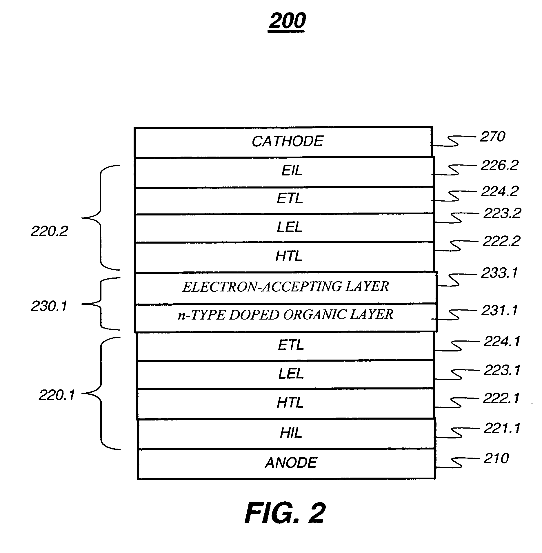
[0135] A tandem OLED of device having two white light-emitting organic EL units was prepared by depositing a first EL unit, a connector, and then a second EL unit over the CFx layer, as described below.

First EL Unit

[0136] a) an HTL, 60 nm thick, including NPB;

[0137] b) a yellow light-emitting layer including 20 nm of NPB doped with 3% Compound 1 (yellow light-emitting dopant) and 20% by volume Compound 2 as stabilizer;

[0138] c) a blue light-emitting layer including 20 nm of Compound 2 with 1% by volume Compound 3 (blue light-emitting dopant) and 6% by volume NPB co-dopant forms a blue emitting layer; and

[0139] d) 5 nm ETL including Alq as the electron-transporting material.

First Connector

[0140] a) 20 nm thick n-type doped organic layer, including 20 nm Bphen as the electron-transporting material doped and doped with 2% by volume Li metal; and

[0141] b) 2 nm tungsten oxide (WOx).

Second EL Unit

[0142] a) an HTL, 60 nm thick, including NPB;

[0143] b) a yellow light...


PUM

PropertyMeasurementUnit
reduction potentialaaaaaaaaaa
work functionaaaaaaaaaa
thicknessaaaaaaaaaa

Abstract

A tandem OLED device includes an anode, a cathode, first and second electroluminescent units disposed between the anode and the cathode, and an intermediate connector disposed between the first and second electroluminescent units. Each of the electroluminescent units include at least one individually selected organic light-emitting layer, and the first electroluminescent unit includes a first electron-transporting layer disposed between the cathode and the light-emitting layer of the first electroluminescent unit, wherein the first electron-transporting layer includes a first electron-transporting material. The intermediate connector includes a first n-type doped organic layer disposed in contact with the first electron-transporting layer, and wherein the first n-type doped organic layer includes an n-type dopant and an electron-transporting material that is different from the first electron-transporting material.

Description

CROSS REFERENCE TO RELATED APPLICATIONS [0001] Reference is made to commonly assigned U.S. patent application Ser. No. 10 / 824,086 filed Apr. 14, 2004 by Michele L. Ricks et al., entitled “OLED Device Using Reduced Drive Voltage,” commonly assigned U.S. patent application Ser. No. 10 / 857,516 filed May 28, 2004 by Liang-Sheng Liao et al., entitled “Tandem OLED Having Stable Intermediate Connectors,” commonly assigned U.S. patent application Ser. No. 10 / 922,606 filed Aug. 20, 2004 by Liang-Sheng Liao et al., entitled “White OLED Having Multiple White Electroluminescence Units,” commonly assigned U.S. patent application Ser. No. 10 / 970,928 filed Oct. 22, 2004 by Liang-Sheng Liao et al., entitled “White OLEDs With a Color Compensated Electroluminescent Unit,” commonly assigned U.S. patent application Ser. No. 10 / 990,865 filed Nov. 17, 2004 by Jeffrey Spindler et al., entitled “Selecting White Point For OLED Devices,” commonly assigned U.S. patent application Ser. No. 10 / 772,867 filed Feb...

Claims


Application Information

Patent Timeline
Patent Type & Authority Applications(United States)
IPC IPC(8): H01L51/50H05B33/00
CPCC09K11/06H01L51/0052H01L51/0059H01L51/0081H05B33/14H01L51/5278H01L2251/305H01L2251/308H01L51/5052H10K85/615H10K85/631H10K85/324H10K50/155H10K50/165H10K50/19H10K2102/101H10K2102/103
Inventor HATWAR, TUKARAM K.LIAO, LIANG-SHENGTYAN, YUAN-SHENGVAN SLYKE, STEVEN A.
Owner EASTMAN KODAK CO
Why Eureka
Try Eureka