Method for manufacturing semiconductor device capable of improving breakdown voltage characteristics

a semiconductor device and breakdown voltage technology, applied in the direction of semiconductor devices, electrical equipment, transistors, etc., can solve the problems of deteriorating breakdown voltage characteristics, and achieve the effect of improving breakdown voltage characteristics

Inactive Publication Date: 2006-10-26
NEC ELECTRONICS CORP
View PDF6 Cites 10 Cited by
  • Summary
  • Abstract
  • Description
  • Claims
  • Application Information

AI Technical Summary

Benefits of technology

[0008] According to the present invention, p-type impurities are introduced into a part of the periphery of the active area adjacent to the element isolation layer that is only beneath the gate electrode. As a result, while the improvement of the sub threshold characteristics is maintained, the breakdown voltage characteristics can be improved.

Problems solved by technology

In the above-described prior art manufacturing method, however, since the p-type impurities are introduced into the entire periphery of the active area adjacent to the element isolation layer, the breakdown voltage characteristics deteriorate.

Method used


Image

  • Method for manufacturing semiconductor device capable of improving breakdown voltage characteristics
  • Method for manufacturing semiconductor device capable of improving breakdown voltage characteristics
  • Method for manufacturing semiconductor device capable of improving breakdown voltage characteristics

Examples


first embodiment

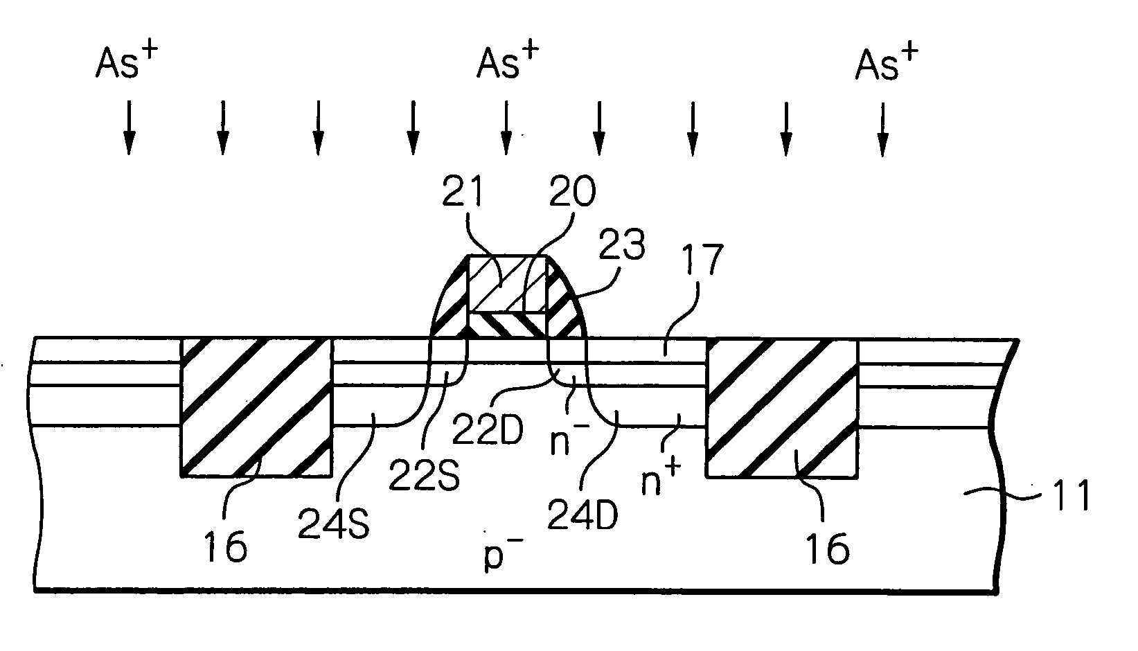
[0052] the method for manufacturing a semiconductor device such as an n-channel MOS transistor will be explained next with reference to FIGS. 6A through 6J.

[0053] First, referring to FIG. 6A, a silicon dioxide layer 12 and a silicon nitride layer 13 are deposited on a p−-type monocrystalline silicon substrate 11. In this case, the silicon dioxide layer 12 can be formed by thermally oxidizing the silicon substrate 11. Then, an opening 14 is perforated in the silicon nitride layer 13 and the silicon dioxide layer 12 by a photolithography and etching process.

[0054] Next, referring to FIG. 6B, the silicon substrate 11 is etched by using the silicon nitride layer 13 and the silicon dioxide layer 12 as a mask. As a result, a trench (groove) 15 is formed within the silicon substrate 11.

[0055] Next, referring to FIG. 6C, a silicon dioxide layer 16 is buried in the trench 15 of the silicon substrate 11 and the opening 14 of the silicon nitride layer 13 and the silicon dioxide layer 12 by a...

second embodiment

[0070] the method for manufacturing a semiconductor device such as two CMOS circuits will be explained next with reference to FIGS. 10A through 10J. In this case, one CMOS circuit is a low breakdown voltage CMOS circuit formed by one n-channel MOS transistor Qn1 and one p-channel MOS transistor Qp1 powered by 3.3V, and the other CMOS circuit is a high breakdown voltage CMOS circuit formed by one n-channel MOS transistor Qn2 and one p-channel MOS transistor Qp2 powered by 5V.

[0071] First, referring to FIG. 10A, an STI layer 32 is formed within a p−−-type monocrystalline silicon substrate 31 in a similar way to those of FIGS. 6A, 6B, 6C and 6D. As a result, element forming areas (active areas) for the transistors Qn1, Qp1, Qn2 and Qp2 are partitioned from each other.

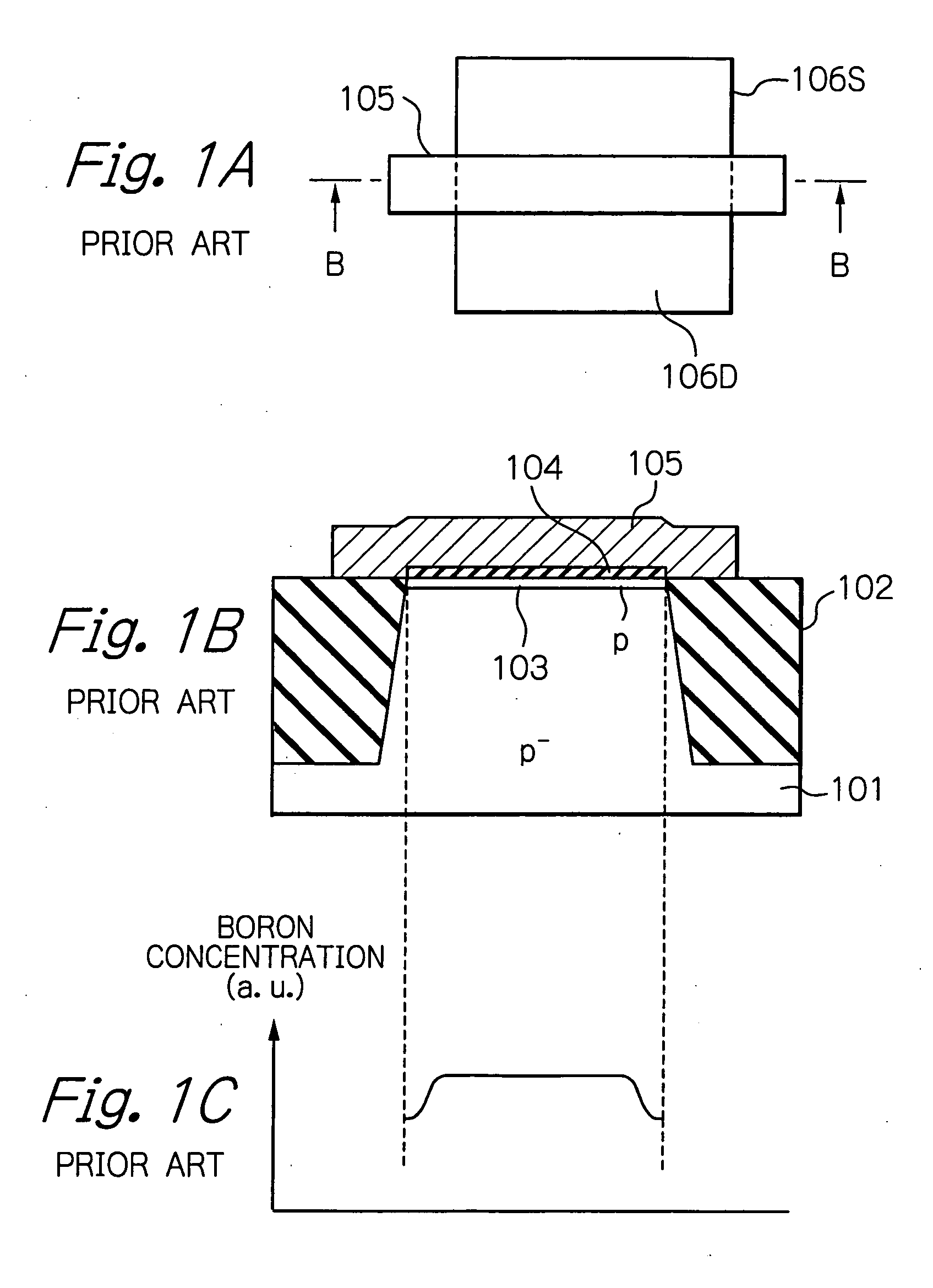
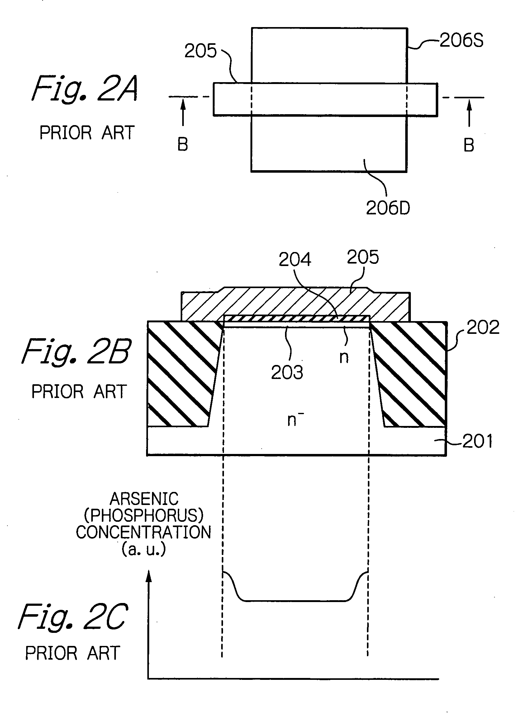
[0072] Next, referring to FIG. 10B, a photoresist pattern layer 33 having an opening 33a corresponding to the n-channel MOS transistor Qn2 is formed on the silicon substrate 31 by a photolithography process. Then, boron i...


PUM


Abstract

In a method for manufacturing a MOS transistor, a MOS transistor isolation layer is formed within a semiconductor substrate to surround an area for forming the MOS transistor in the semiconductor substrate. Then, first impurities are introduced into the area of the semiconductor substrate to adjust a threshold voltage of the MOS transistor. Also, second impurities are introduced into only a part of a periphery of the above-mentioned area adjacent to the MOS transistor isolation layer above which a gate electrode of the MOS transistor will be formed.

Description

BACKGROUND OF THE INVENTION [0001] 1. Field of the Invention [0002] The present invention relates to a method for manufacturing a semiconductor device such as a metal oxide semiconductor (MOS) transistor partitioned by a thick element isolation layer such as a shallow trench isolation (STI) layer or a local oxidation of silicon (LOCOS) layer. [0003] 2. Description of the Related Art [0004] When manufacturing a MOS transistor, impurities are introduced into a silicon substrate under a gate electrode, to thereby adjust the threshold voltage of the MOS transistor. On the other hand, in order to partition MOS transistors from each other, a thick element isolation layer such as an STI layer or a LOCOS layer made of silicon dioxide, has been introduced. [0005] When the width and the length of a channel have been decreased, a so-called narrow channel width effect becomes remarkable. For example, in an n-channel MOS transistor, boron atoms are introduced into a silicon substrate under a gat...

Claims


Application Information

Patent Timeline
Patent Type & Authority Applications(United States)
IPC IPC(8): H01L21/336
CPCH01L21/823412H01L21/823493H01L21/823807H01L29/7833H01L27/0922H01L29/1041H01L29/6659H01L21/823892
Inventor INOUE, TOMOHARU
Owner NEC ELECTRONICS CORP
Why Eureka
Try Eureka