Reconfigurable dielectric waveguide antenna

Active Publication Date: 2006-11-02
SIERRA NEVADA CORP
View PDF7 Cites 182 Cited by
  • Summary
  • Abstract
  • Description
  • Claims
  • Application Information

AI Technical Summary

Benefits of technology

[0009] As will be more readily appreciated from the detailed description that follows, the present invention provides an antenna that can transmit and/or receive electromagnetic radiation in a beam ha

Problems solved by technology

This type of antenna requires a motor and a transmission and control mechanism to rotate the drum in a controllable manner, thereby adding to the weight, size, cost and complexity of the antenna system.
Other approaches to the problem of directing electromagnetic radi

Method used


Image

  • Reconfigurable dielectric waveguide antenna
  • Reconfigurable dielectric waveguide antenna
  • Reconfigurable dielectric waveguide antenna

Examples


second embodiment

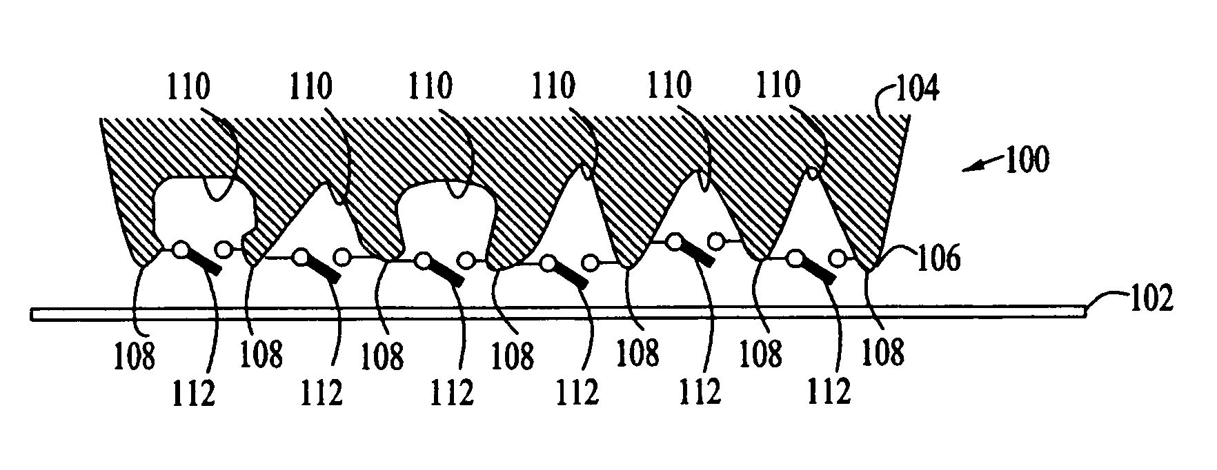
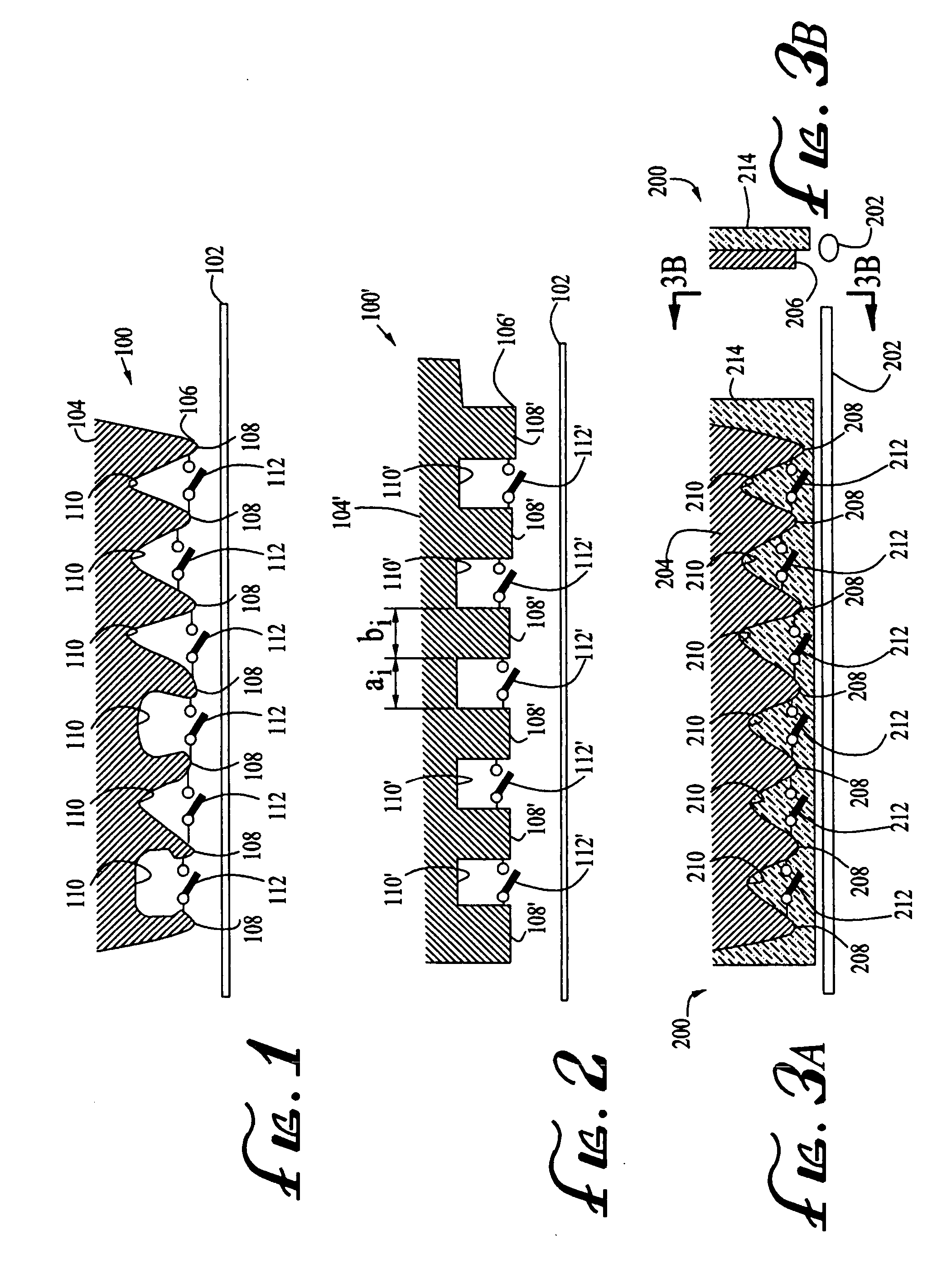
[0036]FIGS. 3A and 3B illustrate an antenna 200, in accordance with the invention, having a transmission line 202, as described above, and a metal antenna plate 204, the latter having an evanescent coupling edge 206 comprising a series of alternating convexities or serrations 208 and concavities or notches 210. As in the previously-described embodiment, each adjacent pair of convexities 208 is selectively connectable by a switch 212.

[0037] In the antenna of FIGS. 3A and 3B, the metal antenna plate 204 is advantageously formed or placed on a substrate 214. The substrate 214 may be a dielectric material, such as quartz, sapphire, ceramic, a suitable plastic, or a polymeric composite. Alternatively, the substrate 214 may be a semiconductor, such as silicon, gallium arsenide, gallium phosphide, germanium, gallium nitride, indium phosphide, gallium aluminum arsenide, or SOI (silicon-on-insulator).

third embodiment

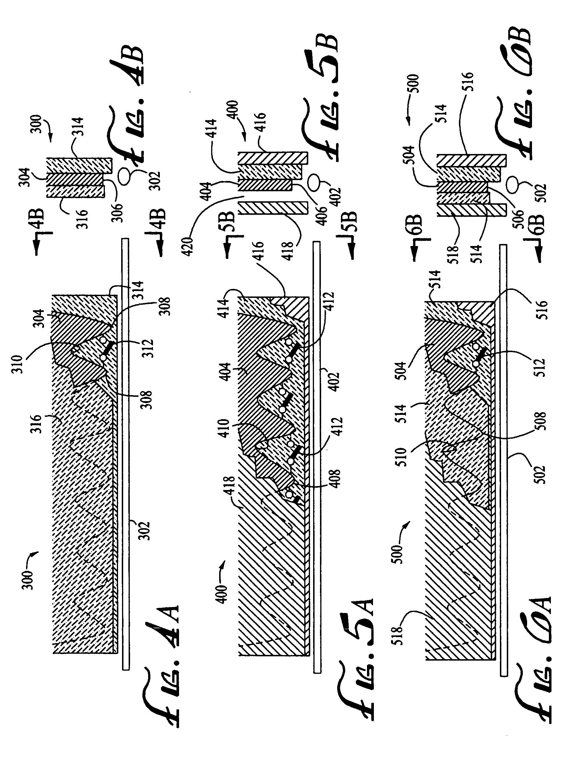
[0038]FIGS. 4A and 4B show an antenna 300 according to the invention, which, like the previously-described embodiments, includes a transmission line 302 and a metal antenna plate 304. The antenna plate 304 has an evanescent coupling edge 306, having convexities 308 separated by concavities 310. Each adjacent pair of convexities 308 is selectively connectable by a switch 312, as discussed above. In this embodiment, the metal antenna plate 304 is sandwiched between a substrate 314 and a cover layer 316. As in the embodiment of FIGS. 3A and 3B, the substrate 314 may be either a dielectric or a semiconductor material. The cover layer 316 is also of a dielectric or semiconductor material, but not necessarily the same material as that of the substrate 314.

fourth embodiment

[0039] An antenna 400 in accordance with the invention is shown in FIGS. 5A and 5B. The antenna 400 includes a transmission line 402 and a metal antenna plate 404. The antenna plate 404 has an evanescent coupling edge 406, having convexities 408 separated by concavities 410. Each adjacent pair of convexities 408 is selectively connectable by a switch 412, as discussed above. In this embodiment, the metal antenna plate 404 is formed on or adhered to the front surface of a dielectric or semiconductor substrate 414, the rear surface of which is attached to a metal backing plate 416. A metal face plate 418 is separated by an air gap 420 from the metal coupling plate 404.


PUM


Abstract

A reconfigurable directional antenna for transmission and reception of electromagnetic radiation includes a transmission line aligned with and adjacent to a metal antenna element with an evanescent coupling edge having a selectively variable electromagnetic coupling geometry. The shape and direction of the beam are determined by the selected coupling geometry of the coupling edge, as determined by the pattern of electrical connections selected for physical edge features of the coupling edge. The electrical connections between the edge features are selected by the selective actuation of an array of “on-off” switches that close and open electrical connections between individual edge features. The selection of the “on” or “off” state of the individual switches thus changes the electromagnetic geometry of the coupling edge, and, therefore the direction and shape of the transmitted or received beam. The actuation of the switches may be accomplished under the control of an appropriately-programmed computer.

Description

CROSS-REFERENCE TO RELATED APPLICATION [0001] Not Applicable FEDERALLY SPONSORED RESEARCH OR DEVELOPMENT [0002] Not Applicable BACKGROUND OF THE INVENTION [0003] This invention relates generally to the field of dielectric waveguide antennas. More specifically, it relates to such antennas that transmit or receive electromagnetic radiation (particularly millimeter wavelength radiation) in selectable directions determined by controllably varying the effective electromagnetic coupling geometry of the antenna. [0004] Dielectric waveguide antennas are well-known in the art, as exemplified by U.S. Pat. No. 6,750,827; U.S. Pat. No. 6,211,836; U.S. Pat. No. 5,815,124; and U.S. Pat. No. 5,959,589, the disclosures of which are incorporated herein by reference. Such antennas operate by the evanescent coupling of electromagnetic waves out of an elongate (typically rod-like) dielectric waveguide to a rotating cylinder or drum, and then radiating the coupled electromagnetic energy in directions de...

Claims


Application Information

Patent Timeline
IPC IPC(8): H01Q13/00
CPCH01Q3/443H01Q23/00H01Q13/28
Inventor AVAKIAN, ARAMAISBRAILOVSKY, ALEXANDERFELMAN, MIKHAILGORDION, IRINAKHODOS, VICTOR V.LITVINOV, VLADIMIR I.MANASSON, VLADIMIRSADOVNIK, LEV
Owner SIERRA NEVADA CORP
Why Eureka
Try Eureka