Method for manufacturing semiconductor device and laser irradiation apparatus

a laser irradiation and semiconductor technology, applied in manufacturing tools, manufacturing tools, instruments, etc., can solve the problems of thermal discontinuous phenomenon, inability to manufacture optical systems with such optical path differences, etc., and achieve the effect of reducing size, simple laser irradiation apparatus, and small laser irradiation apparatus

Inactive Publication Date: 2006-11-02
SEMICON ENERGY LAB CO LTD
View PDF24 Cites 58 Cited by
  • Summary
  • Abstract
  • Description
  • Claims
  • Application Information

AI Technical Summary

Benefits of technology

[0023] In the present invention, a megahertz laser beam is split and an optical path difference equivalent to the length between the pulse width of a megahertz laser beam and the coherence length the split beams, thereby preventing interference between the split beams. Alternatively, a time lag corresponding to the pulse width of a megahertz laser beam or more between the split beams, thereby preventing interference between the split beams. Thus, even a slight optical path difference (time lag) allows a uniform thermal energy distribution of an object to be irradiated without optical interference. Consequently, there are advantages that an optical system for providing an optical path difference can also be reduced in size, and a laser irradiation apparatus can be made smaller.
[0024] When the repetition rate is set at 10 MHz or more, heat can be continuously applied to a semiconductor film, which allows continuous crystal growth. Further, when the pulse width is 1 ns or less, an optical path difference between the split beams can be 10 cm or less, so that an optical system which can be practically designed can be manufactured. In addition, when the pulse width is 100 fs or more, the structure of the. laser apparatus can be made simple, which is industrially advantageous.
[0025] In the case of a megahertz laser beam having a repetition rate of 10 MHz or more and a pulse width of 100 fs to 1 ns, when the length correspond

Problems solved by technology

For example, in the case of a laser beam emitted from a solid-state laser, the coherence length reaches several meters to several kilometers; thus, it has been impractical to manufacture an optical system provided with such an optical path difference.
Further, in

Method used


Image

  • Method for manufacturing semiconductor device and laser irradiation apparatus
  • Method for manufacturing semiconductor device and laser irradiation apparatus
  • Method for manufacturing semiconductor device and laser irradiation apparatus

Examples


embodiment mode 1

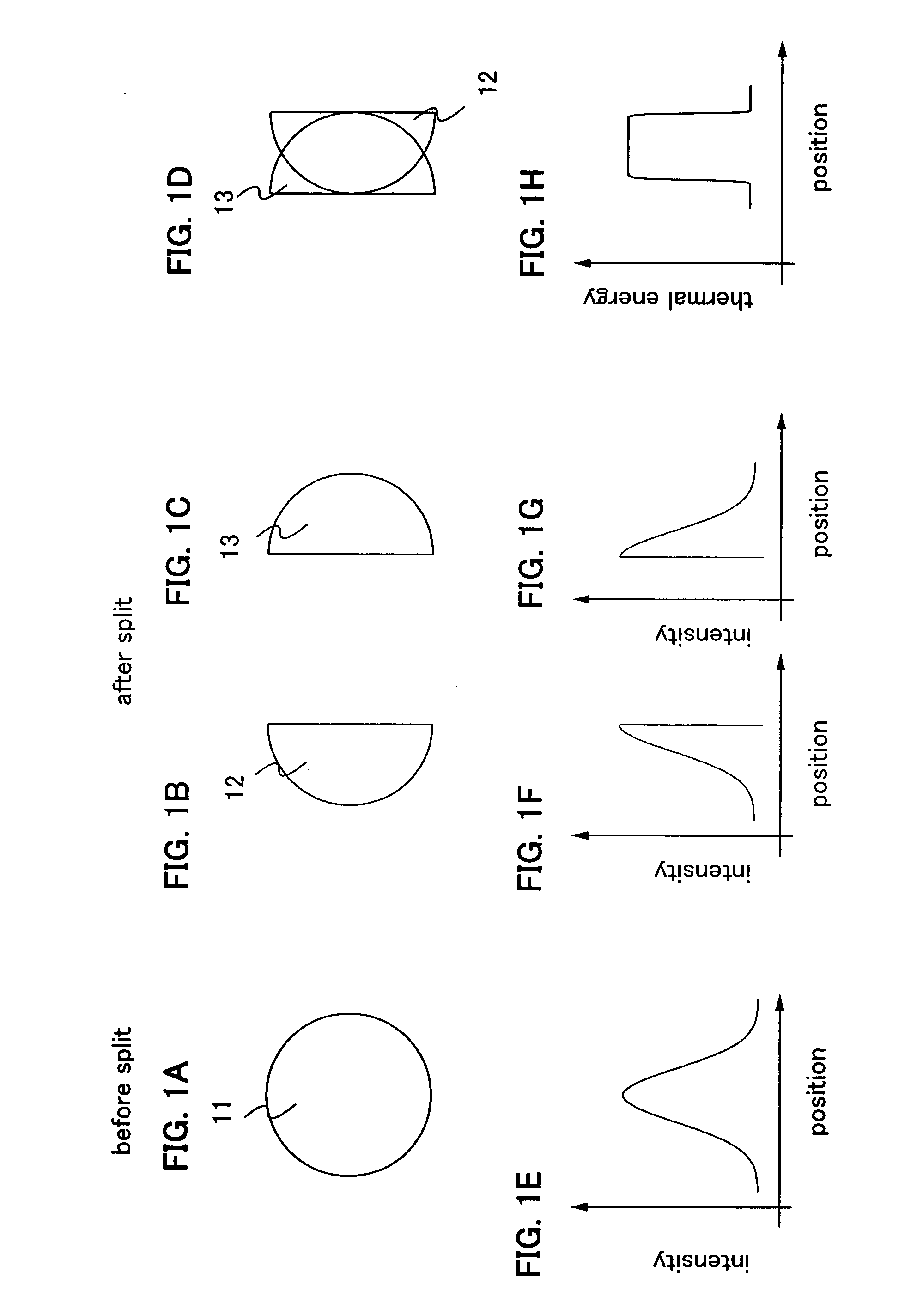
[0050]FIGS. 1A to 1H show shapes of a beam cross section of a megahertz laser beam which has been split and supplied to a common portion of an object to be irradiated in different periods respectively, intensity distributions and thermal energy distributions. FIG. 1A shows the beam cross section of a megahertz laser beam before splitting, FIG. 1B and FIG. 1C show beam cross sections of megahertz laser beams being split, and FIG. 1D shows the beam cross section of a megahertz laser beam supplied to the common portion of the object to be irradiated in different periods respectively. FIG. 1E shows the intensity distribution of the beam cross section before splitting, FIGS. 1F and 1G shows the intensity distribution of the split beam cross section of the split beams, FIG. 1H shows the thermal energy distribution which is supplied to the common portion applied with the split beams in different periods respectively. Here, a megahertz laser beam is split into two beams; however, it may be ...

embodiment mode 2

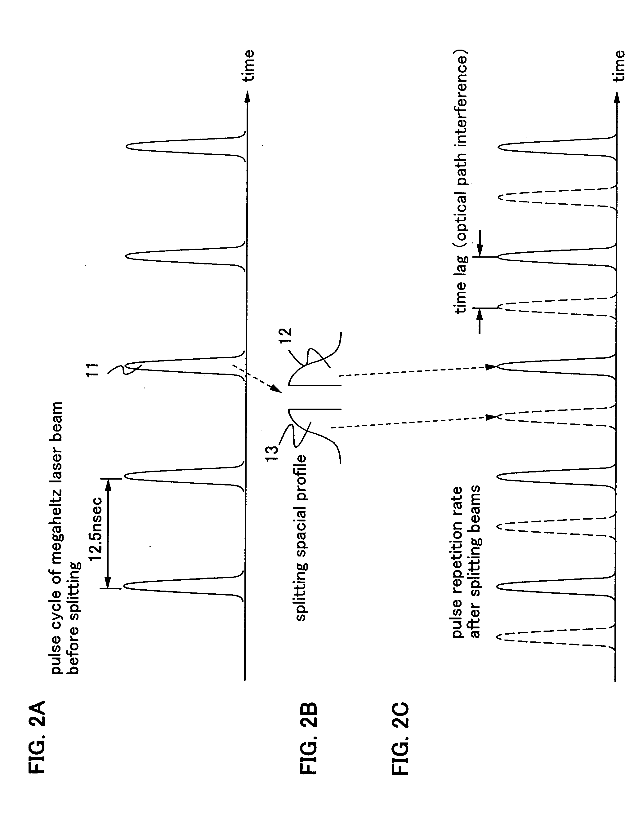
[0063] In this embodiment mode, a mode in which an object to be irradiated over a glass substrate or a quartz substrate is irradiated with a laser beam will be described. In the case where an object to be irradiated is over a glass substrate or a quartz substrate, a laser beam which is not absorbed by the object to be irradiated may be reflected by the back face of the substrate and delivered again to the object to be irradiated. In that case, behavior of the light reflected from the back face of the substrate is necessarily considered when the optical path difference is determined to prevent the optical interference. In this embodiment mode, wetting of the optical path difference in consideration of light reflected by the back face of the substrate will be described with reference to FIG. 3A to FIG. 4D. Note that the time lag td is less than a repetition interval of 1 / N of the laser beam. It is because when the pulse repetition is set at the pulse repetition interval of the laser b...

embodiment 1

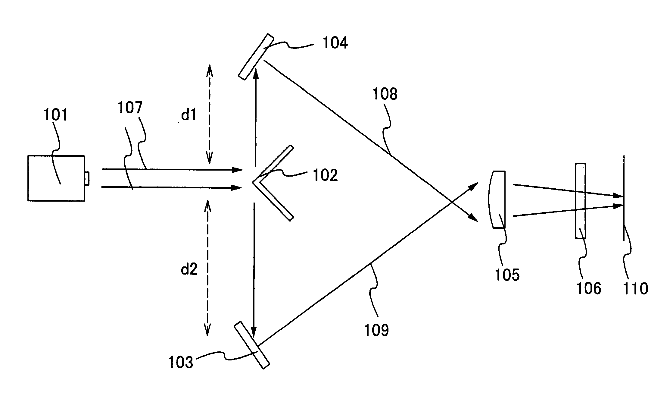
[0092] In Embodiment 1, a laser irradiation apparatus of the present invention will be described. FIG. 5A shows a laser irradiation apparatus, FIG. 5B shows a shape of a beam cross section before splitting, FIGS. 5C and 5D show shapes of cross sections of split beams, and FIG. 5E shows a cross section of the split beams applied to a common portion of a surface to be irradiated in different periods respectively. FIG. 5F shows intensity distribution of a cross section of a beam before splitting, FIGS. 5G and 5H each show intensity distribution of a cross section split beams, and FIG. 5I shows thermal energy distribution of the surface to be irradiated with the split beams in different periods respectively.

[0093] In FIG. 5A, a laser beam 107 emitted from a laser oscillator 101 is split into a first laser beam 108 and a second laser beam 109 by a splitter. The laser beams 107, 108, and 109 are megahertz laser beams. As the splitter 102 a split mirror is used. The laser beam 107 has a c...


PUM

PropertyMeasurementUnit
Timeaaaaaaaaaa
Timeaaaaaaaaaa
Frequencyaaaaaaaaaa

Abstract

It is an object to achieve continuous crystal growth without optical interference using a compact laser irradiation apparatus. A megahertz laser beam is split and combined to crystallize a semiconductor film. At this point of time, an optical path difference is provided between the split beams to reduce optical interference. The optical path difference is set to have a length equivalent to the pulse width of the megahertz laser beam or more and less than a length equivalent to the pulse repetition interval; thus, optical interference can be suppressed with a very short optical path difference. Therefore, laser beams can be applied continuously and efficiently without energy deterioration.

Description

BACKGROUND OF THE INVENTION [0001] 1. Field of the Invention [0002] The present invention relates to a method for manufacturing a semiconductor device by laser irradiation and to a laser irradiation apparatus. [0003] 2. Description of the Related Art [0004] Laser irradiation is generally used in manufacturing a semiconductor device. As one of the reasons, as compared with an annealing method using radiant heating or conductive heating, the treatment time can be reduced substantially. As another reason, the laser irradiation does not thermally damage a substrate which is easily deformed by heat, such as a glass substrate. [0005] However, a beam cross section of a laser beam has energy intensity distribution (hereinafter also referred to as intensity distribution), so that an object to be irradiated could not have been irradiated with a laser beam at a uniform intensity. For example, in the case of crystallizing an object to be irradiated by laser annealing, it has been impossible to ...

Claims


Application Information

Patent Timeline
IPC IPC(8): H01L21/36B23K26/00G06K19/07G06K19/077H01L21/20H01L21/268H01L21/336H01L21/84H01L29/786H01L51/50H05B33/10H05B33/14H05B44/00
CPCH01L27/1266H01L27/3244B23K26/0039B23K26/0608H01L27/1285B23K26/067B23K26/0738B23K2201/40H01L21/2026B23K26/0635B23K26/0006B23K26/0624B23K2101/40B23K2103/50H01L21/02686H01L21/02678H01L21/02422H01L21/02488H01L21/02532H01L21/02505H01L21/0242H01L21/02672H01L21/02691H10K59/12
Inventor TANAKA, KOICHIROOISHI, HIROTADA
Owner SEMICON ENERGY LAB CO LTD
Why Eureka
Try Eureka