

Transient pulse, substrate-triggered biCMOS rail clamp for ESD abatement
a technology of bicmos rail clamps and transient pulses, applied in the direction of transistors, emergency protective arrangements for limiting excess voltage/current, electrical appliances, etc., can solve problems such as failure of integrated circuit operation, current leakage, and internal damage to integrated circuits
- Summary
- Abstract
- Description
- Claims
- Application Information
AI Technical Summary
Benefits of technology
Problems solved by technology
Method used
Image

Examples
Embodiment Construction
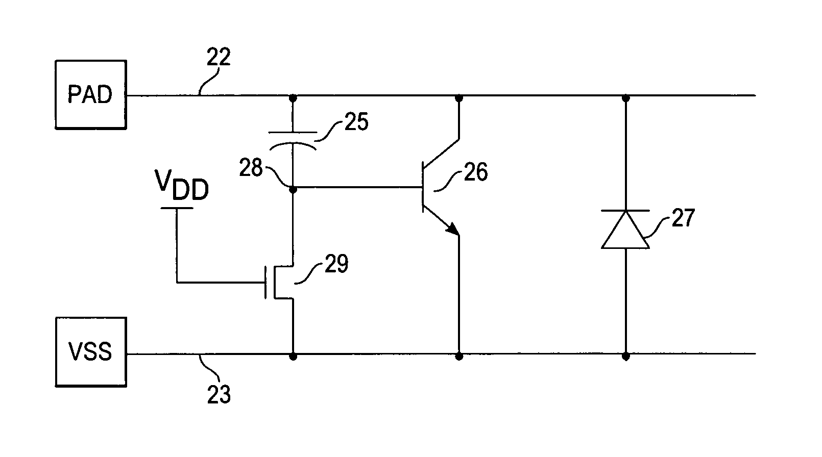
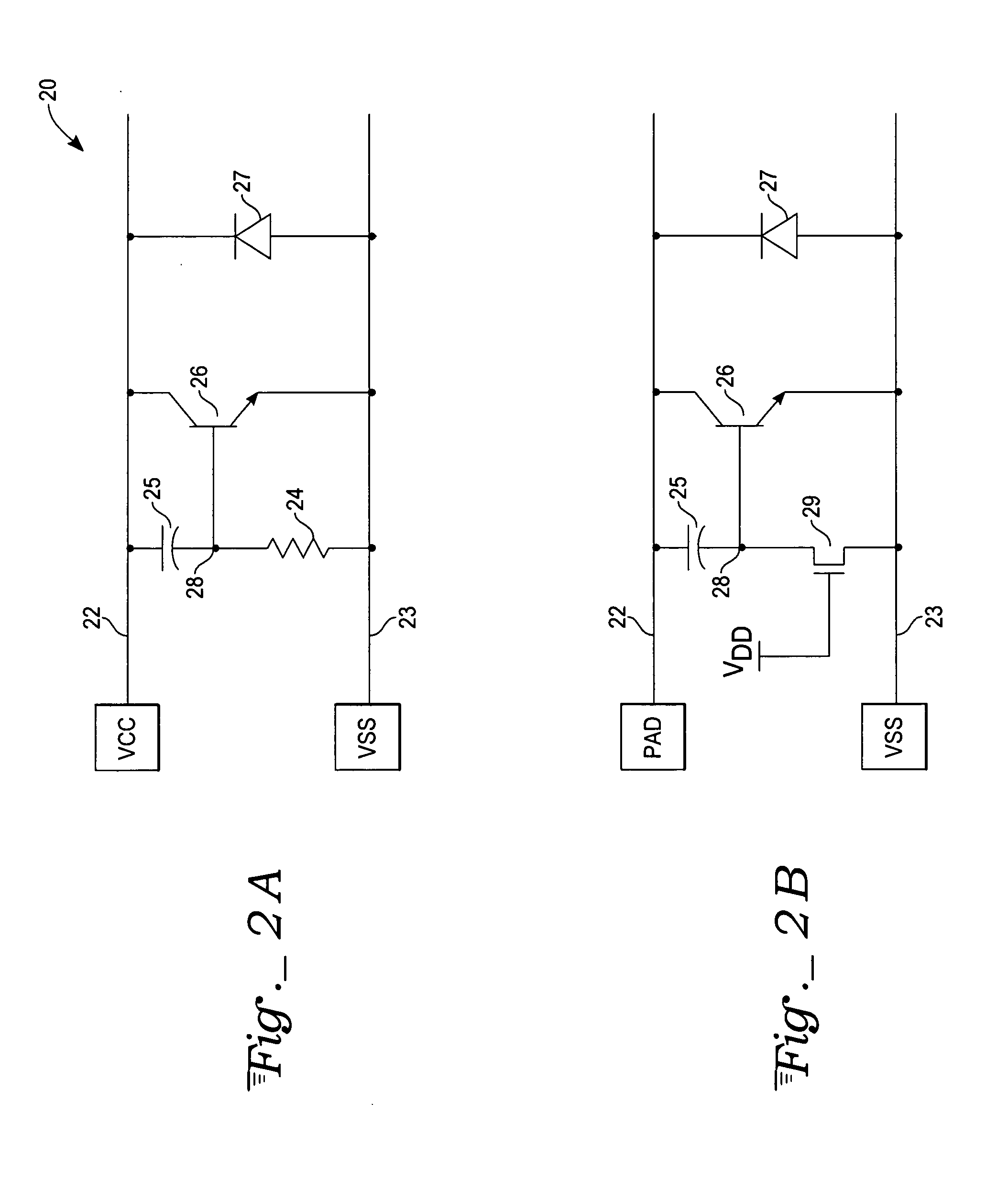
[0012] Referring to FIG. 2A, a voltage supply line 22 and a voltage reference line 23 or ground line provides voltage and power for an integrated circuit configured as an exemplary over-voltage protection circuit 20. A first terminal of a capacitor 25 is electrically coupled to the voltage supply line 22, and a second terminal of the capacitor 25 is electrically coupled to a first node 28. A first terminal of a resistor 24 is electrically coupled to the first node 28, and a second terminal of the resistor 24 is electrically coupled to the voltage reference line 23.
[0013] A single bipolar npn transistor 26 having a collector, emitter, and base, is electrically coupled to the voltage supply line 22, the voltage reference line 23, and the first node 28. The collector of the transistor 26 is electrically coupled to the voltage supply line 22, the emitter of the transistor 26 is coupled to the voltage reference line 23, and the base of the transistor 26 is electrically coupled to the fi...
PUM
 Abstract
Description
Claims
Application Information