Conductive barrier layer, especially an alloy of ruthenium and tantalum and sputter deposition thereof

Inactive Publication Date: 2006-11-09
APPLIED MATERIALS INC
View PDF21 Cites 77 Cited by
  • Summary
  • Abstract
  • Description
  • Claims
  • Application Information

AI Technical Summary

Benefits of technology

[0024] A noble copper alloy seed layer may be formed of copper and one the Group VIIIB elements except iron. Ruthenium copper is the preferred noble copper alloy. The alloying percentages may be freely

Problems solved by technology

One challenging application in the fabrication of advanced integrated circuits is to sputter deposit thin liner layers in vertical electrical interconnects, usually called vias, for copper metallization.
However, copper cannot directly contact the dielectric layer 66.
Copper does not adhere well to oxide.
Copper also can diffuse into the upper-level dielectric layer 66 and cause it to lose its insulating characteristics and short out the devices being formed.
As will be discussed later, the copper continuity has become a major issue.
However, future generations of integrated circuits will present increasing difficulty as the width of the via hole 68 shrinks below current widths at the 90 nm node toward much smaller widths at the 32 nm node (via widths of 50 nm are forecast for the metal-1 level at the 32 nm node) while the thickness of the dielectric layer 66 remains close to 1 μm.
Several problems arise from the increasing aspect ratio of the holes.
There is some diffusion of the copper up and down the sidewall, but it is insu

Method used


Image

  • Conductive barrier layer, especially an alloy of ruthenium and tantalum and sputter deposition thereof
  • Conductive barrier layer, especially an alloy of ruthenium and tantalum and sputter deposition thereof
  • Conductive barrier layer, especially an alloy of ruthenium and tantalum and sputter deposition thereof

Examples


Embodiment Construction

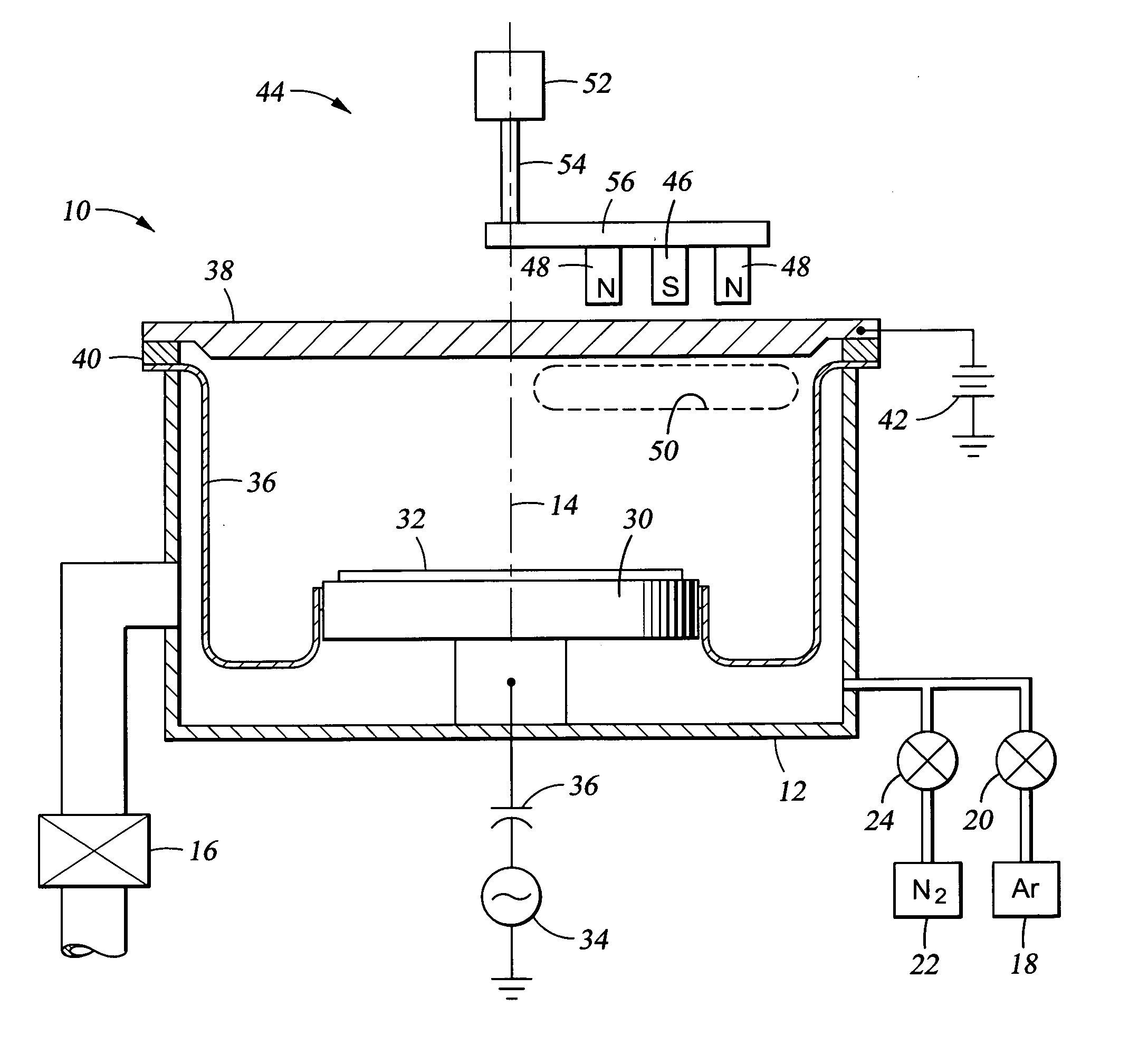
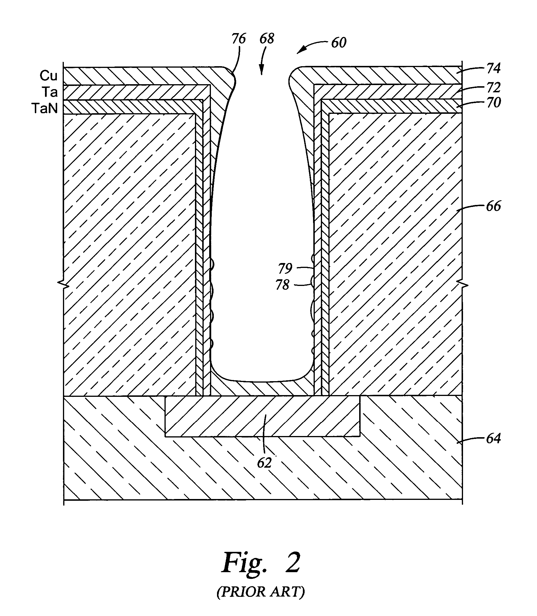
[0032] A first embodiment of a novel copper interconnect liner structure 80 is illustrated in the cross-sectional view of FIG. 3. A barrier layer 82 of an alloy of ruthenium and tantalum is deposited directly over the upper-level dielectric layer 66 and onto the sidewalls of the via hole 68. The RuTa alloy is but one type of a refractory noble alloy to be discussed later. A refractory noble alloy is a metal so it is electrically conductive and can be deposited by magnetron sputtering using a target of the desired alloy composition. A copper seed layer 84 is deposited over the RuTa barrier layer 82 to serve as a plating electrode and as a seed for the copper filled into the remaining portion of the via hole 68 by electrochemical plating (ECP). The excess copper deposited above the top of the via hole 68 is thereafter removed by chemical mechanical polishing (CMP).

[0033] This structure provides several advantages. The ruthenium content may be sufficiently high that the RuTa alloy doe...


PUM

PropertyMeasurementUnit
Structureaaaaaaaaaa
Electrical conductoraaaaaaaaaa
Refractoryaaaaaaaaaa

Abstract

A fabrication method, a product structure, a fabrication method, and a sputtering target for the deposition of a conductive barrier or other liner layer in an interconnect structure. The barrier layer comprises a conductive metal of a refractory noble metal alloy, such as a ruthenium/tantalum alloy, which may be amorphous though it is not required to be so. The barrier layer may be sputtered from a target of similar composition. The barrier and target composition may be chosen from a combination of the refractory metals and the platinum-group metals as well as RuTa. A copper noble seed layer may be formed of an alloy of copper and ruthenium in contact to a barrier layer over the dielectric.

Description

FIELD OF THE INVENTION [0001] The invention relates generally to electrical interconnects including a barrier layer in semiconductor integrated circuits. In particular the invention relates to conductive metal barriers that are not subject to oxidation, such as amorphous metal barriers, or are conductive when oxidized and their sputter deposition. BACKGROUND ART [0002] Sputtering, alternatively called physical vapor deposition (PVD), is the most prevalent method of depositing layers of metals and related materials in the fabrication of silicon integrated circuits. One challenging application in the fabrication of advanced integrated circuits is to sputter deposit thin liner layers in vertical electrical interconnects, usually called vias, for copper metallization. A conventional magnetron sputter reactor 10, illustrated schematically in cross section in FIG. 1, with different targets can effectively sputter thin films of Cu, Ta, TaN, and other materials into holes having high aspect...

Claims


Application Information

Patent Timeline
IPC IPC(8): B32B3/00
CPCB32B15/018C23C14/3414Y10T428/24917H01L21/76844H01L23/53238H01L21/2855H01L2924/0002H01L2924/00H01L21/203H01L21/28
Inventor WANG, JENN YUEWANG, WEI D.WANG, RONJUNTANAKA, YOICHIROCHUNG, HUAZHANG, HONGYU, JICKGOPALRAJA, PRABURAMFU, JIANMING
Owner APPLIED MATERIALS INC
Why Eureka
Try Eureka