
Method for the production of an anti-reflecting surface on optical integrated circuits

Inactive Publication Date: 2006-11-09
INFINEON TECH AG
View PDF14 Cites 12 Cited by
  • Summary
  • Abstract
  • Description
  • Claims
  • Application Information

AI Technical Summary

Benefits of technology

[0011] The invention is based on the object, then, of providing a method for the production of an anti-reflecting surface for optical integrated circuits that can be realized with little complexity and hence low costs and is compatible with IC and single device technologies.

Problems solved by technology

The disadvantage of these layers, however, is that they are optimized for a specific wavelength and are thus unsuitable for multispectral applications.
However, this method has particular disadvantages in combination with the photodiode integrated into a chip technology.
In particular, the realization of multiple layers means that process costs are multiplied correspondingly in comparison with a single layer deposition.
Moreover, this increases the throughput time in production, thereby causing an obstructive build-up at the respective coating installations (bottleneck effect).
Moreover, it is difficult to realize the required accuracy of the layers to layer thicknesses of a few nanometers.
Furthermore, in semiconductor fabrication, the required refractive indices of light cannot be realized or are not available.
In the case of ARC layers, in particular in the case of multilayers, a certain attenuation of the incident light is unavoidable.
However, the production of inverted pyramids of this type is associated with a considerable complexity, so that this variant is not suitable for a practical application.

Method used


Image

  • Method for the production of an anti-reflecting surface on optical integrated circuits
  • Method for the production of an anti-reflecting surface on optical integrated circuits

Examples


Embodiment Construction

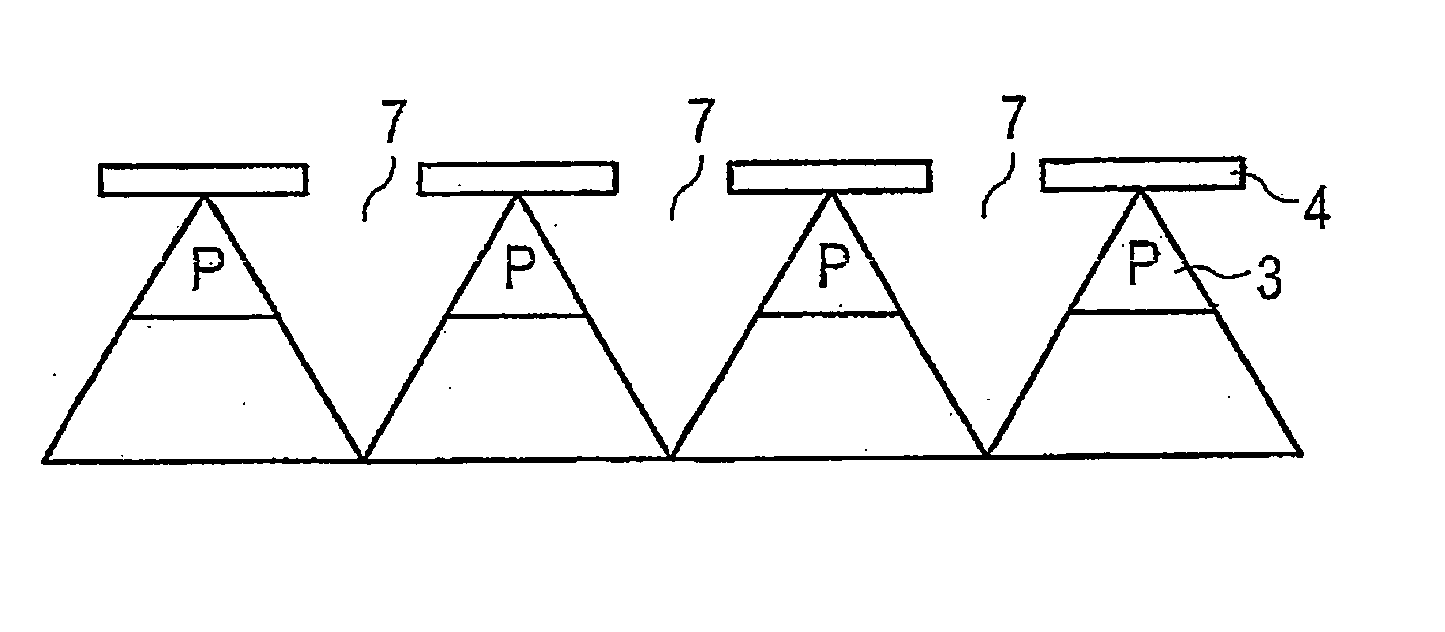
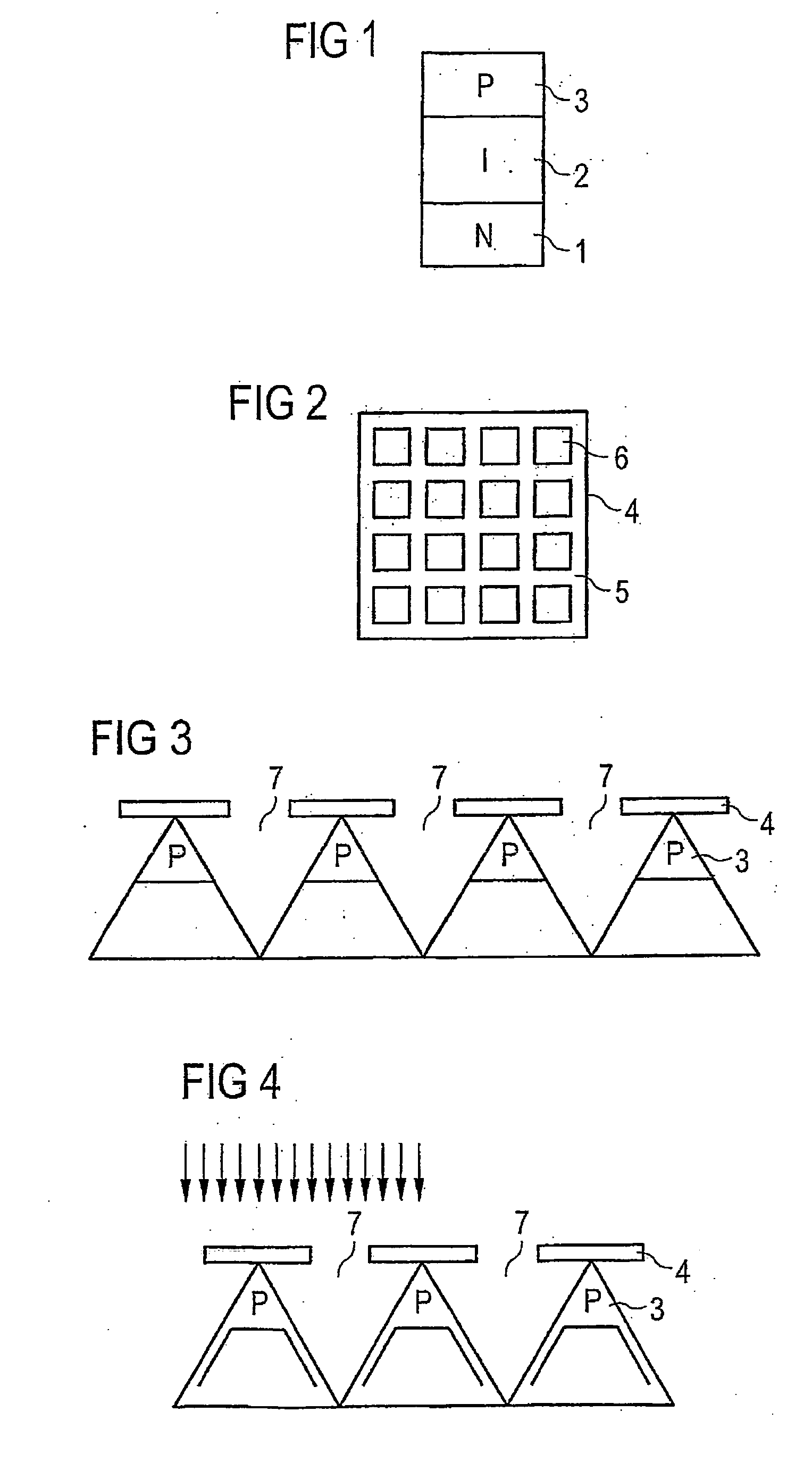
[0029]FIG. 1 shows the basic construction of a photodetector comprising a cathode 1 (n-region), an intrinsic region 2 (i-region) and an anode 3 (p-region) arranged thereabove. This structure is produced on a substrate, for example a silicon substrate, by arsenic implantation, epitaxy and boron implantation. This structure is part of a wafer that is large in areal terms and has been provided with a hard mask 4 by means of an SiO2 deposition and subsequent photolithography. The hard mask 4 may be patterned by customary dry etching, thus giving rise to webs 5 having a width of 0.3 μm to 1 μm and mesh openings 6 having a width 0.5 μm to 5 μm (FIG. 2).

[0030] A structure etching step is subsequently performed, preferably by means of anisotropic, wet-chemical etching, and produces depressions (trenches) having a depth of approximately 1.5 μm that are arranged in regularly distributed fashion and have acuter angles than pyramids with (111) faces, or preferably inverse pyramids 7 (FIG. 3). ...


PUM


Abstract

A photodetector is formed in a semiconductor body. A hard mask grating is photolithographically formed on a surface of the semiconductor body. The semiconductor body is etched using the hard mask grating as a mask. The etching is performed down to a predetermined depth. An implantation is performed such that an anode or cathode of the photodector that has been interrupted during the etching is re-formed.

Description

[0001] This application is a continuation of co-pending International Application No. PCT / DE2004 / 002340, filed Oct. 20, 2004, which designated the United States and was not published in English, and which is based on German Application No. 102 50 643.8, filed Oct. 29, 2003, both of which applications are incorporated herein by reference.TECHNICAL FIELD [0002] The invention relates to a method for the production of an anti-reflecting surface on optical integrated circuits in order to improve the absorption of light in photodetectors. BACKGROUND [0003] Photodetectors of this type, such as PIN photodiodes, comprise a cathode (n-region), an insulation (i-region) and an anode (p-region). This structure is produced on a substrate, for example a silicon substrate, by means of a first implantation, epitaxy and a second implantation. [0004] In order to achieve good light absorption in a desired wavelength range, simple ARC layers (anti-reflecting coating) are deposited on the photodiode, or ...

Claims


Application Information

Patent Timeline
IPC IPC(8): G03C5/00H01L31/0216H01L31/0232H01L31/0236H01L31/18
CPCH01L31/0236Y02E10/547H01L31/1804H01L31/02363Y02P70/50
Inventor WILLE, HOLGERLANGGUTH, GERNOTMUELLER, KARL-HEINZ
Owner INFINEON TECH AG
Learn More