Unlock instant, AI-driven research and patent intelligence for your innovation.

Reactive codoping of gaalinp compound semiconductors

a technology of reacting codoping and compound semiconductors, which is applied in the direction of chemically reactive gases, crystal growth process, polycrystalline material growth, etc., can solve the problems of difficult to achieve high p-type conductivity, heavy p-type doping of gaalinp compound semiconductors with high al content, such as alinp, and difficult to achieve single acceptors

Inactive Publication Date: 2006-11-09
ALLIANCE FOR SUSTAINABLE ENERGY
View PDF11 Cites 3 Cited by
  • Summary
  • Abstract
  • Description
  • Claims
  • Application Information

AI Technical Summary

Benefits of technology

[0005] The present invention additionally further includes a method of producing a GaAlInP compound semiconductor. The method comprises the steps of disposing a GaAs single crystal as a substrate in a metal organic vapor deposition reactor, preparing Al, Ga, In vapors by thermally decomposing organometallic compounds of Al, Ga, and In, preparing P vapors by thermally decomposing phosphine gas, preparing group II element vapors by thermally decomposing an organometallic group IIA or IIB compound, preparing group VIB vapors by thermally decomposing a gaseous compound of group VIB, simultaneously supplying the Al, Ga, In, P, group II, and group VIB vapors to a region for epitaxial crystal growth on the substrate, and epitaxially growing a GaAlInP crystal doped with group IIA or IIB and group VIB elements on said substrate wherein the group IIA or IIB and group VIB vapors supplied to the region for epitaxial crystal growth produce a codoped GaAlInP compound semiconductor with a group IIA or IIB element serving as a p-type dopant having low group II atomic diff

Problems solved by technology

For some semiconductor materials, it is difficult to obtain high p-type conductivity because of the solubility, activation, and diffusion dynamics of the materials in question.
Heavy p-type doping of GaAlInP compound semiconductors with high Al content, such as AlInP, is difficult to achieve with single acceptor species such as Zn, Mg, or Be.

Method used


Image

  • Reactive codoping of gaalinp compound semiconductors
  • Reactive codoping of gaalinp compound semiconductors
  • Reactive codoping of gaalinp compound semiconductors

Examples


example 1

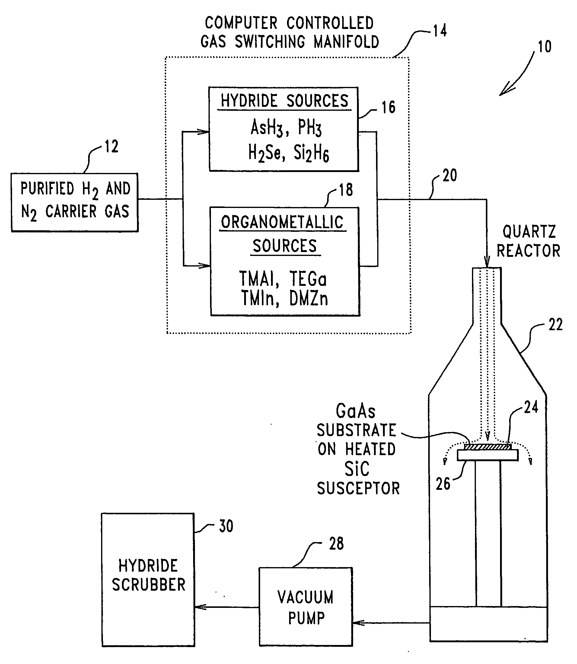
[0021] A GaAs single crystal with a 511A crystallographic orientation was used as a substrate for the growth of an AlInP single crystal and was located in a metal organic chemical vapor deposition (MOCVD) reactor held at seventy-five (75) torr. AlInP single crystals closely lattice matched to the GaAs were epitaxially grown at temperatures of 540° C.-600° C. by supplying 0.4 sccm of trimethylaluminum, 0.22 sccm of trimethylindium, and 250 sccm of phosphine in ten (10) slm of hydrogen carrier gas. Zn doping was accomplished by introducing dimethylzinc at flow rates of 0.32 to 3.2 sccm. Se doping was accomplished by introducing a gas mixture consisting of 100 ppm of H2Se in hydrogen at flow rates of two (2) to one hundred (100) sccm. Various combinations of Zn doped only and Zn+Se codoped AlInP crystals were grown. The atomic Zn and Se concentrations, NZn and NSe, respectively, were measured by secondary ion mass spectroscopy (SIMS) and are summarized in Table 1. In the AlInP crystal ...

example 2

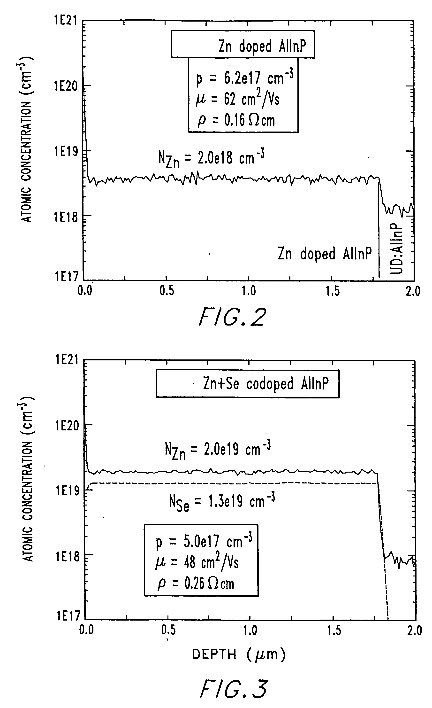
[0022] A GaAs single crystal with a 511A crystallographic orientation was used as a substrate for the growth of an AlInP single crystal and was located in a metal organic chemical vapor deposition (MOCVD) reactor at held seventy-five (75) torr. Zn doped only and Zn+Se codoped AlInP single crystals closely lattice matched to the GaAs were epitaxially grown on an undoped AlInP buffer layer at temperature of 600° C. by supplying 0.4 sccm of trimethylaluminum, 0.22 sccm of trimethylindium, and 250 sccm of phosphine in ten (10) slm of hydrogen carrier gas. Zn doping was accomplished by introducing dimethylzinc at flow rate of 1.6 sccm. Se doping was accomplished by introducing a gas mixture consisting of 100 ppm of H2Se in hydrogen at a flow rate of ten (10) sccm. The profiles of atomic Zn and Se concentrations, NZn and NSe, respectively, in Zn doped only and Zn+Se codoped AlInP single crystals were measured by secondary ion mass spectroscopy (SIMS) and are illustrated in FIGS. 2 and 3, ...

example 3

[0023] A GaAs single crystal with a 511A crystallographic orientation was used as a substrate for the growth of an AlInP single crystal and was located in a metal organic chemical vapor deposition (MOCVD) reactor at held seventy-five (75) torr. Very heavily Zn doped AlInP single crystals closely lattice matched to the GaAs were epitaxially grown at temperature of 540° C. by supplying 0.4 sccm of trimethylaluminum, 0.22 sccm of trimethylindium, and 400 sccm of phosphine in ten (10) slm of hydrogen carrier gas. Zn doping was accomplished by introducing dimethylzinc at a flow rate of 0.32 sccm. Se doping was accomplished by introducing a gas mixture consisting of 100 ppm of H2Se in hydrogen at a flow rate of one hundred (100) sccm. The profiles of atomic Zn and Se concentrations, NZn and NSe, respectively, in Zn doped only and Zn+Se codoped AlInP single crystals were measured by secondary ion mass spectroscopy (SIMS) and are illustrated in FIG. 4 and FIG. 5, respectively. At these high...


PUM


Abstract

A GaAlInP compound semiconductor and a method of producing a GaAlInP compound semiconductor are provided. The apparatus and method comprises a GaAs crystal substrate in a metal organic vapor deposition reactor. Al, Ga, In vapors are prepared by thermally decomposing organometallic compounds. P vapors are prepared by thermally decomposing phospine gas, group II vapors are prepared by thermally decomposing an organometallic group IIA or IIB compound. Group VIB vapors are prepared by thermally decomposing a gaseous compound of group VIB. The Al, Ga, In, P, group II, and group VIB vapors grow a GaAlInP crystal doped with group IIA or IIB and group VIB elements on the substrate wherein the group IIA or IIB and a group VIB vapors produced a codoped GaAlInP compound semiconductor with a group IIA or IIB element serving as a p-type dopant having low group II atomic diffusion.

Description

CONTRACTUAL ORIGIN OF THE INVENTION [0001] The United States Government has rights in this invention under Contract No. DE-AC36-99GO10337 between the United States Department of Energy and the National Renewal Energy Laboratory, a division of the Midwest Research Institute.TECHNICAL FIELD [0002] This invention relates generally to a GaAlInP compound semiconductor and the production of GaAlInP compound semiconductors and, more particularly, it relates to reactive codoping of GaAlInP compound semiconductors for improved electrical conductivity and dopant stability in heavily doped layers. BACKGROUND ART [0003] Semiconductor devices, such as solar cells and LEDs, require regions with differing types (n-type or p-type) and levels of conductivity. Adding impurity atoms, known as dopants, either to add or remove free electrons, varies the conductivity of the semiconductor device. For some semiconductor materials, it is difficult to obtain high p-type conductivity because of the solubility...

Claims


Application Information

Patent Timeline
IPC IPC(8): H01L21/28H01L21/3205H01L21/4763C30B25/02H01L21/20H01L21/205
CPCC30B25/02C30B29/40H01L21/02395H01L21/0262H01L21/02543H01L21/02576H01L21/02579H01L21/02433
Inventor HANNA, MARK COOPERREEDY, ROBERT
Owner ALLIANCE FOR SUSTAINABLE ENERGY