Composite multi-layer substrate and module using the substrate

a multi-layer substrate and substrate technology, applied in the direction of printed circuit manufacturing, printed circuit non-printed electric components association, printed circuit aspects, etc., can solve the problems of inconvenient mounting of electronic components, processing costs of grooves or holes, disadvantages of thin-sizing substrates, etc., to increase manufacturing costs and increase electrical properties.

Inactive Publication Date: 2006-11-16
TAIYO YUDEN KK
View PDF9 Cites 36 Cited by
  • Summary
  • Abstract
  • Description
  • Claims
  • Application Information

AI Technical Summary

Benefits of technology

[0028] In a composite multi-layer substrate which has these characteristics, in order to have a core member which has rigidity, it is not necessary to use glass cloth as a reinforcing material. Therefore, various kinds of inco

Problems solved by technology

However, the first prior art example and the fourth prior art example have a drawback of being disadvantageous to thin-sizing the substrate.
Also, in the second prior art example and the third prior art example, there is a drawback mentioned which involves the processing cost of the grooves or holes.
Moreover, because electronic component heat dissipation countermeasures are not entirely taken into consideration, any of the prior art examples (first through fourth prior art examples) have a drawback causing inconvenience in mounting electronic components especially in regard to heat generation in larger semiconductor chips, etc.
However, by this prior art example, when performing a resin seal of the semiconductor chip and multi-layering, there is a drawback of having to grind off the excess resin requiring additional work and making manufacturing costs more expensive.
Additionally, concerning mounting in a hole and electronic component having multiple electrodes, such as the five-sided electrode, etc., there is a drawback that the type of electronic component which can be mounted has limitations and this constitution was not taken into consideration at all.
However, in this prior art example, the relationship between the-metal foil in the side walls of the holes for mounting semiconductor chips or the height of the metal sheet and the thickness of the semiconductor chips is not defined.
Further, from the depth relationship of the holes for mounting semiconductor chips and the thickness of the semiconductor chips not being clear, consideration of thin-sizing is regarded to be insufficient.
Also, from having to remove the glass cloth (described later) when the holes for mounting semiconductor chips in a printed circuit board are formed, the increased manufacturing cost is readily anticipated.
S64-012598

Method used


Image

  • Composite multi-layer substrate and module using the substrate
  • Composite multi-layer substrate and module using the substrate
  • Composite multi-layer substrate and module using the substrate

Examples


first embodiment

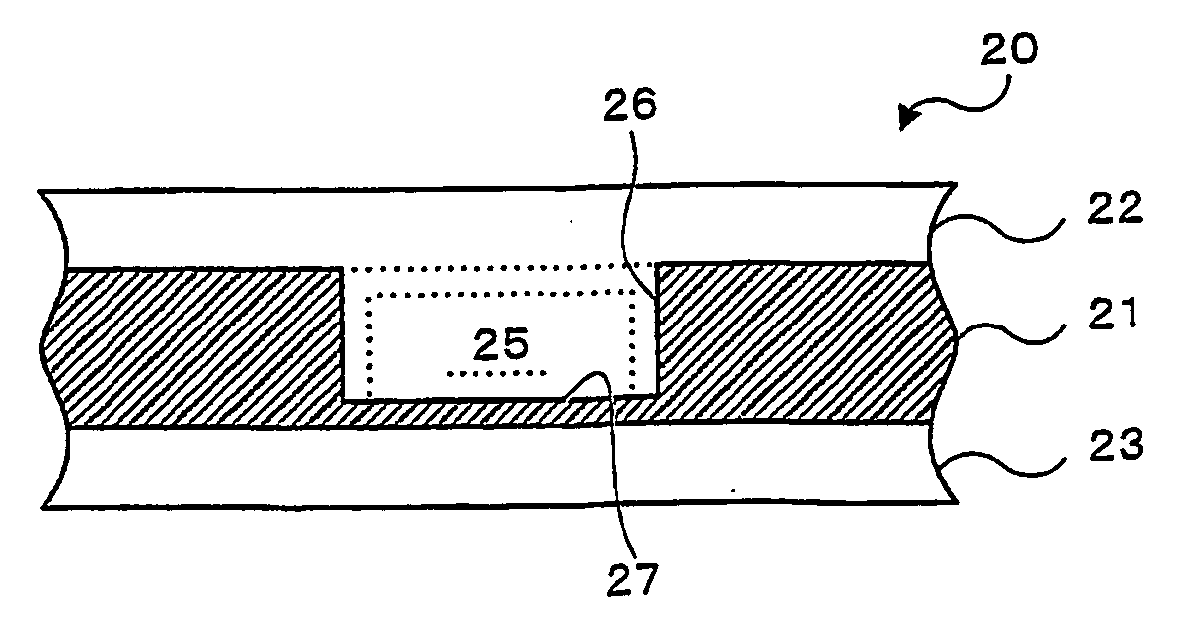
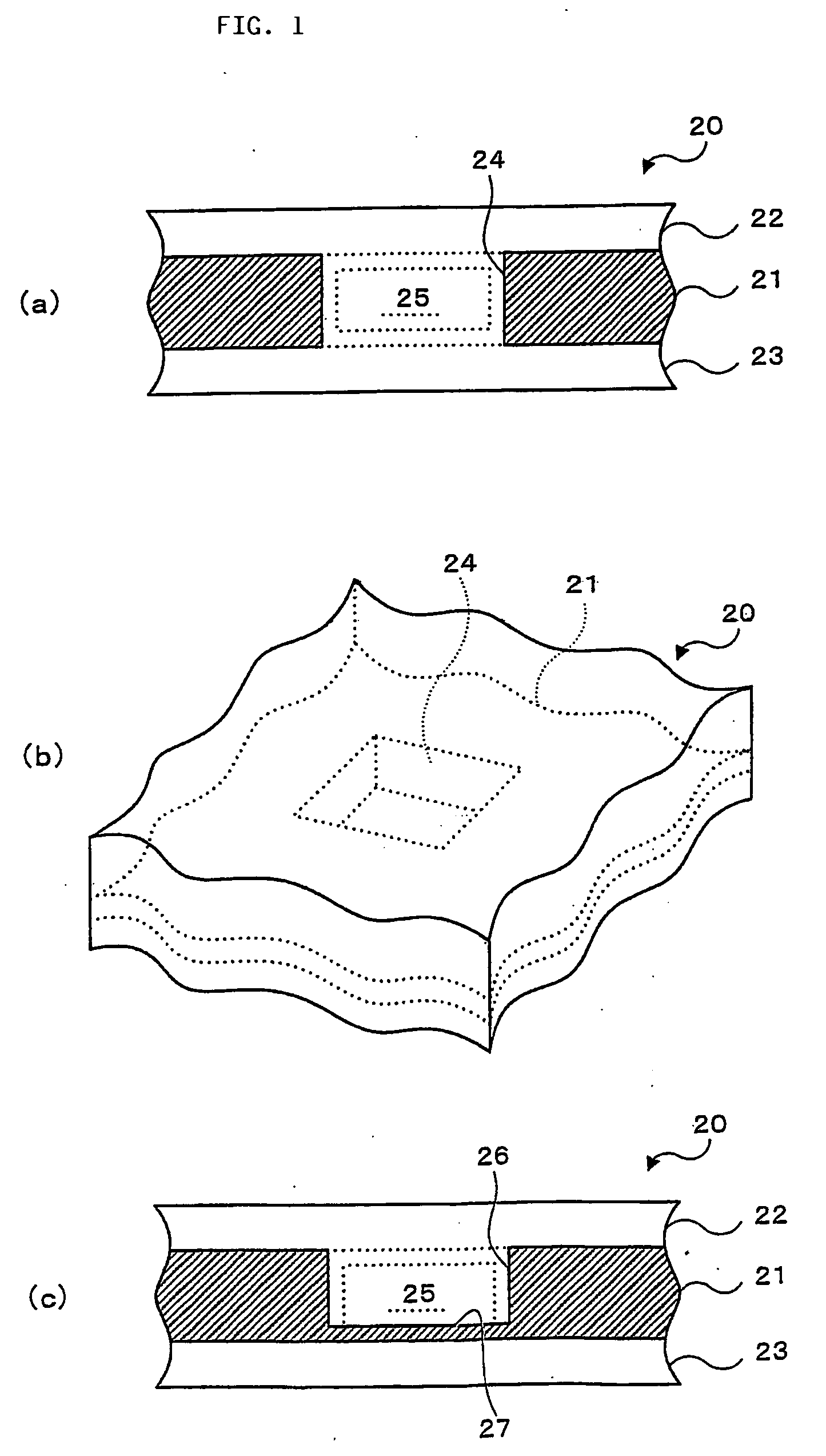
[0050] FIGS. 1A˜1C are main cross sectional plan views and a main perspective view of a composite multi-layer substrate in the form of the embodiment. In this cross sectional view, the composite multi-layer substrate 20 has a “multi-layer structure.” Referring to the example illustration, the composite multi-layer substrate 20 has a three-layer structure comprising a core member 21, a resin layer 22 (hereinafter “substrate front side resin is layer”) and a resin layer 23 (hereinafter “substrate rear side resin layer.” The core member 21 in the shape of a flat plate-like board is composed of a material which has excellent electrical conductivity, excellent heat conductivity and high rigidity. The substrate front side resin layer 22 covers the front surface of the core member 21 (in the direction of the drawing, the upper surface). The substrate rear side resin layer 23 covers the rear surface of the core member 21 (in the direction of the drawing, the lower surface).

[0051] The essen...

second embodiment

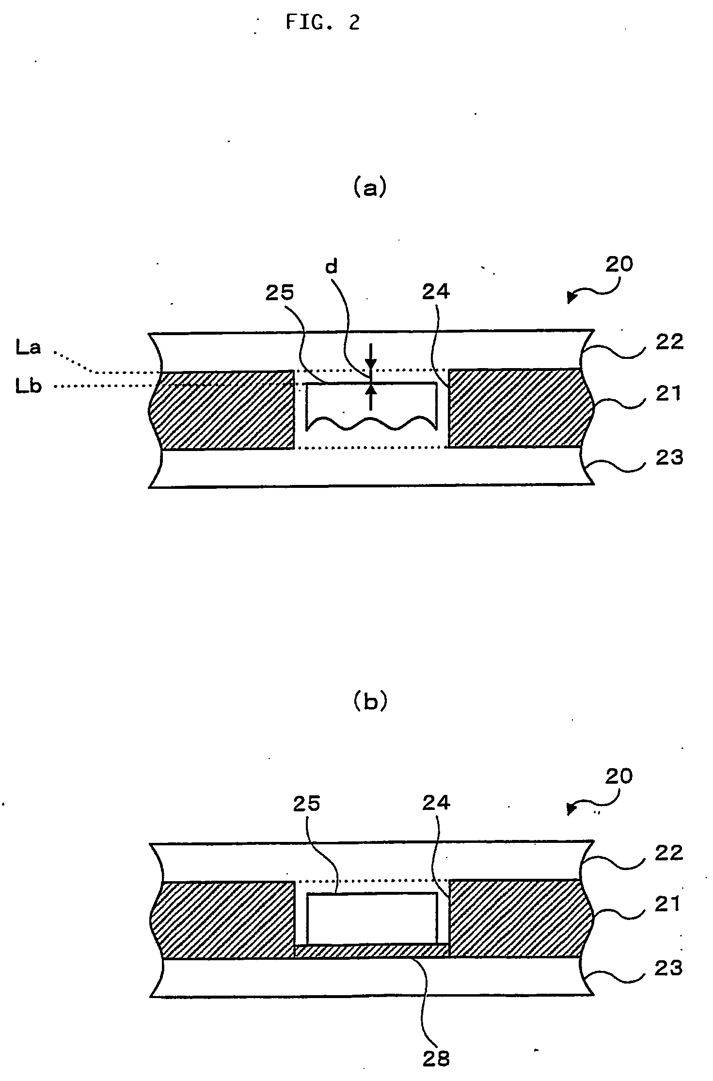
[0059]FIGS. 2A and 2B are composition diagrams when mounting an electronic component 25 in a bottomless hole 24 of the core member 21. Referring to FIG. 2A, when the upper surface height position of the core member 21 is assumed to be La and the upper surface height position of an electronic component 25 is assumed to be Lb, as for the differential d (d=La−Lb) of the height, it is desirable to formulate a value of zero or more than zero (namely, La=Lb or any relation of La>Lb). In this manner, since the upper surface height position La of the core member 21 constitutes a position always higher than the upper surface height position Lb of an electronic component 25, it can respond to the loading (load added when the front side resin layer 22, etc. is laminated) to an electronic component 25 on the core member 21 at the time of manufacturing the composite multi-layer substrate 20 and damage to an electronic component 25 is avoidable.

[0060]FIG. 2B is a composition diagram when mountin...

third embodiment

[0066]FIGS. 4A and 4B is a main cross sectional plan view in another section of the core member 21 and an external perspective view of the section. Referring to these drawings, a column segment 33 is set in an optional position (although adjacent to a bottomless hole 24 in the drawing, it is not limited to this) of the core member 21.

[0067] The column segment 33 is originally a portion of the core member 21. Specifically, it is a “remaining part” of the core member 21 produced by having formed a cylindrical dividing groove 34 in an optional position of the core member 21. A column segment 33 can be used as follows. Namely, when a via hole 35, 36 is formed in both the front side resin layer 22 and the rear side resin layer 23 and an electrode 37, 38 is formed in the via hole 35, 36 in both directions of one end side and the other end side of the column segment 33 (island-shaped sections), the electrode 37, 38 are electrically connected via a column segment 33. Furthermore, because t...


PUM


Abstract

A composite multi-layer substrate comprising a flat plate-like core member formed of a material having an excellent electric conductivity, an excellent heat conductivity, and a high rigidity, a front resin layer and a rear resin layer covering at least the front and rear surfaces of the core member, and a bottomless hole formed in the core member through the front and rear sides of the core member, wherein an electronic component is installed in the bottomless hole, whereby since the strength of the composite multi-layer substrate can be assured by the rigidity of the core member, conventional prior art glass cloth can be eliminated, deterioration in the electric characteristics caused by ion migration can be avoided and will result in reduced production cost.

Description

BACKGROUND OF THE INVENTION [0001] 1. Field of the Invention [0002] This invention relates to a composite multi-layer substrate and module usings a substrate designed to make high density mounting of electronic components feasible. [0003] 2. Description of the Prior Art [0004] Conventionally, package miniaturization has been vigorously carried out as the approach for high density mounting of electronic components. For example, recently the Chip Size Package (CSP) and ultimately bare chip mounting which makes the package itself redundant have been realized. However, each of these is premised on arranging and mounting (flat surface mounting method) a plurality of electronic components in a two-dimensional (surface) array. By simple calculation, the fundamental limitation of not being able to reduce the mounting surface areas to less than the size of the added area of each electronic component is retained. [0005] Therefore, a mounting method using embedded mounting of the electronic co...

Claims


Application Information

Patent Timeline
IPC IPC(8): H01L23/02H01L23/498H05K3/46H01L23/538H05K1/02H05K1/18H05K3/44
CPCH01L23/49822H01L2924/014H01L24/18H01L24/82H01L2224/18H01L2924/01004H01L2924/01027H01L2924/01029H01L2924/01033H01L2924/01057H01L2924/01078H01L2924/01082H01L2924/14H01L2924/19041H01L2924/19042H01L2924/19043H01L2924/30105H01L2924/30107H01L2924/3025H05K1/021H05K1/185H05K3/445H05K3/4641H05K2201/0969H05K2201/09745H01L2924/01005H01L2924/01006H01L2924/01019H01L2924/01037H01L23/5389H01L2924/181H01L2924/12042H01L2224/04105H01L2224/73267H01L2224/92244H01L2924/15153H01L2924/15159H01L2924/19105H01L2224/32225H01L2224/2518H01L2224/32245H01L24/19H01L2924/00
Inventor MIYAZAKI, MASASHITAKAYAMA, MITSUHIROSAWATARI, TATSURO
Owner TAIYO YUDEN KK
Why Eureka
Try Eureka