

Laminate for printed circuit board and method of manufacturing the same
a technology of printed circuit board and laminate, which is applied in the direction of transportation and packaging, synthetic resin layered products, other domestic articles, etc., can solve the problems of non-uniform volume contraction, brittleness and warpage of packaging substrate, delamination and warpage of final products, etc., and achieves low stiffness
- Summary
- Abstract
- Description
- Claims
- Application Information
AI Technical Summary
Benefits of technology
Problems solved by technology
Method used
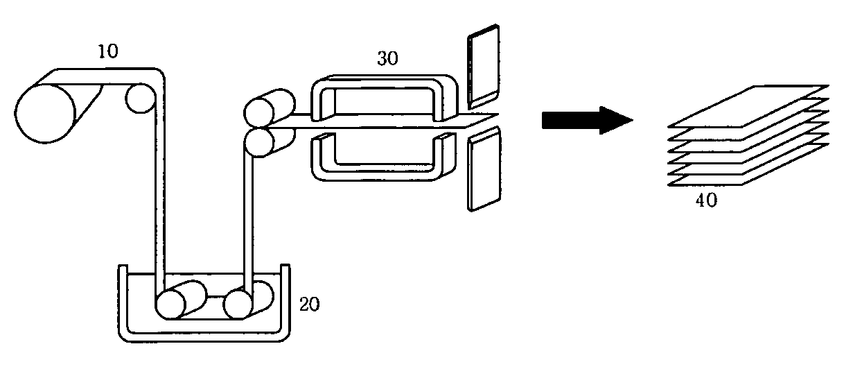
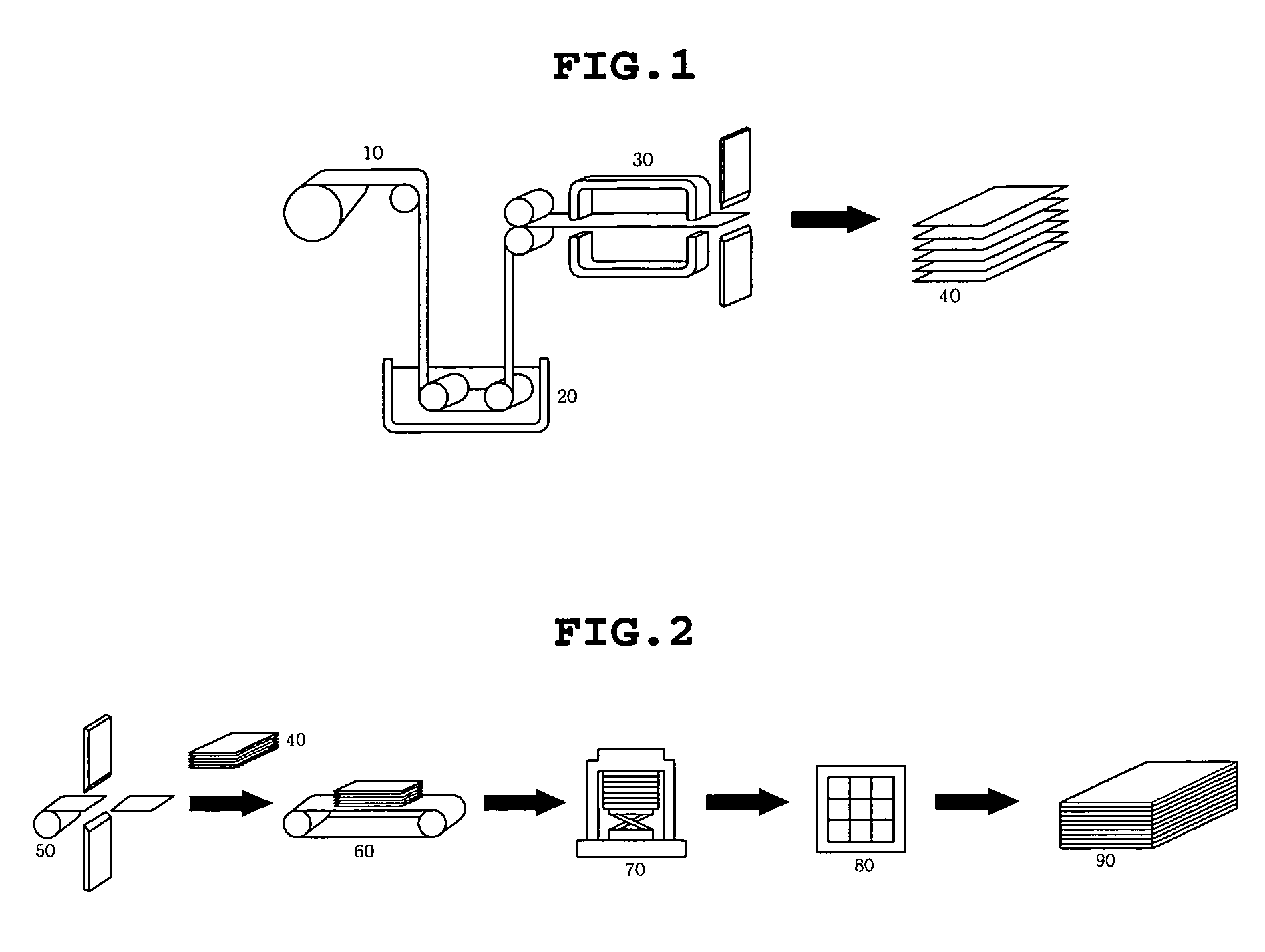
Image

Examples
example 1
[0067] 10 parts by weight of a liquid crystal polyester resin having a liquid crystal melting point of about 300° C. was dissolved in 100 parts by weight of N-methyl pyrrolidone as a solvent, to prepare a liquid crystal polyester solution. Into the solution thus prepared, nonwoven fabric (VECRUS, available from Kuraray) formed of liquid crystal polyester fibers, having an average thickness of about 10 μm, a dielectric constant of 2.8 and a liquid crystal melting point of about 330° C., was incorporated at room temperature for about 8 min. The incorporated nonwoven fabric was pre-dried at about 100° C. for about 1 hr in a nitrogen atmosphere, heated and compressed along with a copper foil at about 250° C. for 2 hr, heat treated and then completely dried, to manufacture a CCL of the present invention. The dielectric constant, dissipation factor, coefficient of thermal expansion, and water absorption rate of the CCL thus manufactured were measured. The results are given in Table 2 belo...
PUM
| Property | Measurement | Unit |
|---|---|---|
| melting point | aaaaa | aaaaa |
| melting point | aaaaa | aaaaa |
| thickness | aaaaa | aaaaa |
Abstract
Description
Claims
Application Information