

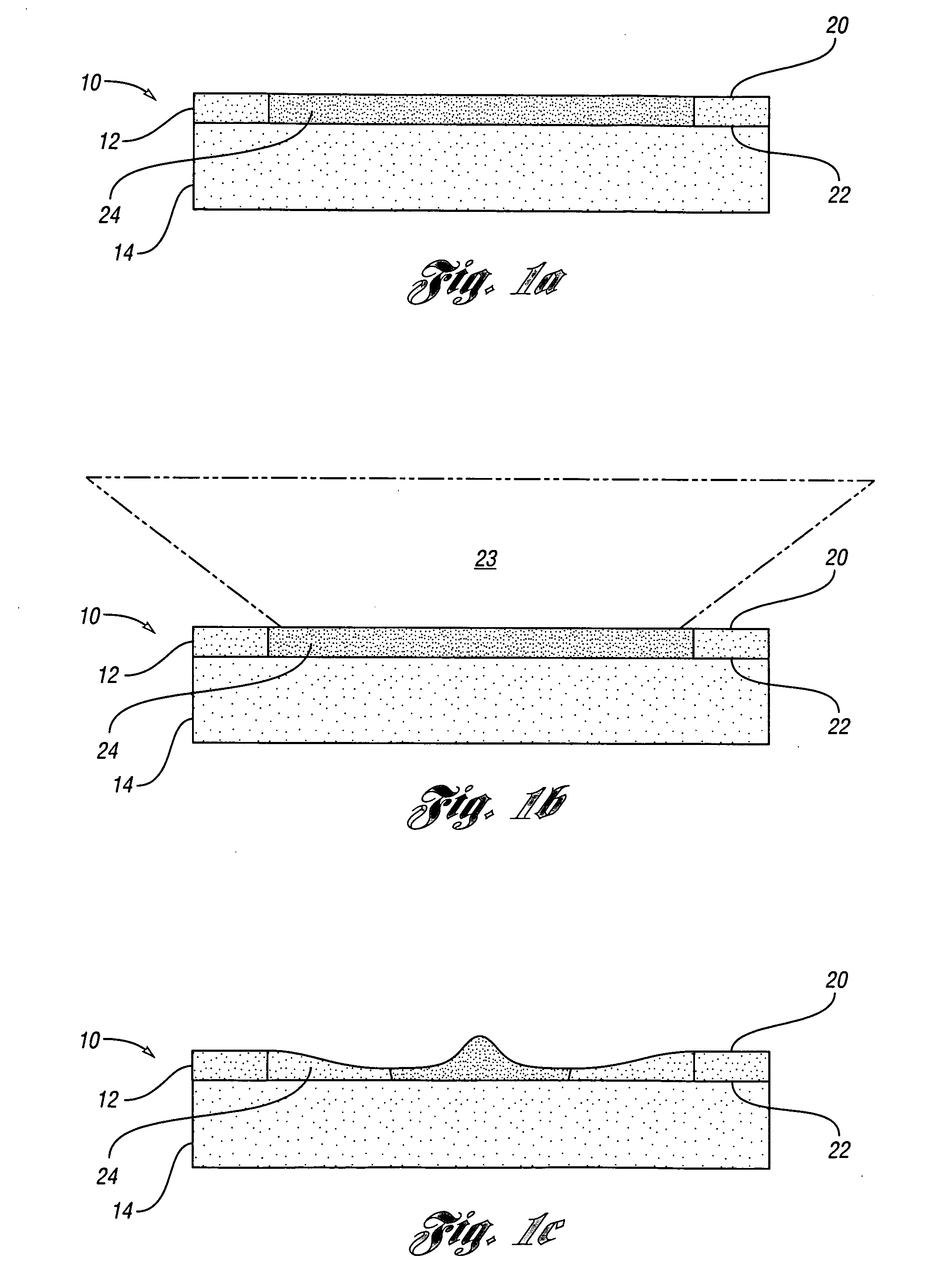
Method of forming micro-structures and nano-structures
a technology of nano-structures and nano-tips, which is applied in the manufacture of micro-structural devices, nanotechnology, electric devices, etc., can solve the problems of non-equilibrium and relatively complex current processes involved in such radiation interactions
- Summary
- Abstract
- Description
- Claims
- Application Information
AI Technical Summary
Benefits of technology
Problems solved by technology
Method used
Image

Examples
example 1
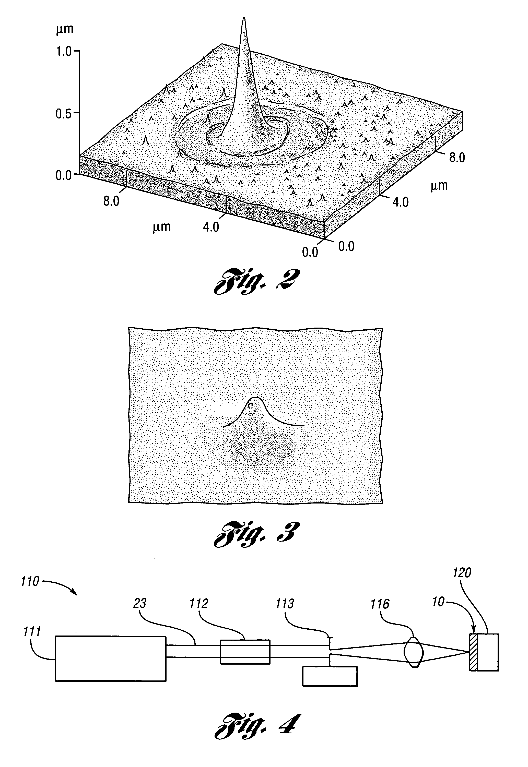
[0046] This example provides a method of forming a nano-structure having a nano-tip for enhanced electron extraction. In this example, spatially homogenized, single pulses of radiation from a KrF excimer laser (λ=248 nm, Lambda Physik, model LPX 205) were used to image pinholes onto uniformly illuminated circular spots on a silicon sample surface. This was accomplished via a projection system with a demagnification factor of 8.9 and a resolution limit of 2 micrometers. Irradiation was performed on commercially acquired silicon-on-insulator (SOI) wafers comprising 200 nm single-crystal silicon (Si) bonded to a silica glass substrate.
[0047] In addition, SOI wafers that comprised of a single-crystal Si layer on 1 μm layer of silica on a bulk Si substrate (SOIS) were used. The samples were plasma-etch-thinned to different thicknesses of the Si layer in the range of between about 0.8 and 4.1 μm. The laser processing was performed in ambient, clean-room conditions, and the sample surface...
example 2
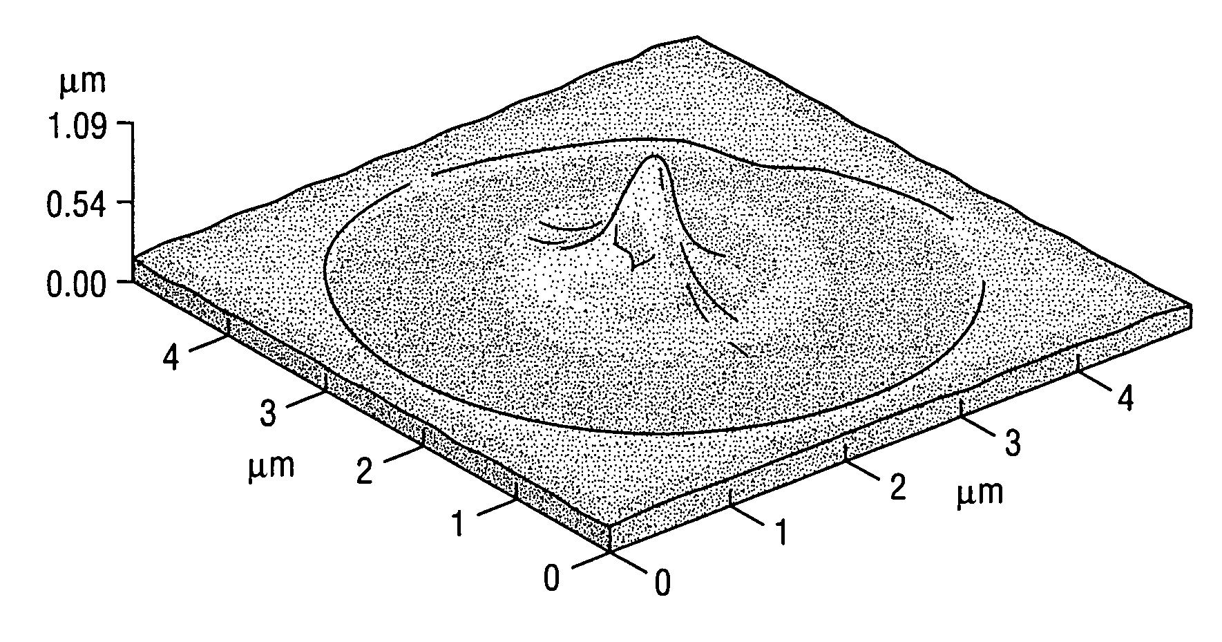
[0051] In this example, fabrication of nano-structures was attempted on SOIS samples with Si film thicknesses of about 0.8 μm, 1.1 μm, 2.3 μm and 4.1 μm. When using a 50 μm pinhole projection mask, there were no observable changes on the surfaces of the films with thicknesses of between about 2.3 and 4.1 μm after single-pulse irradiation with fluences up to 3.0 J / cm2. In the 0.8 μm and 1.1 μm film thickness cases, thresholds were measured to be about 1.5 and 1.75 J / cm2, respectively. FIGS. 8-10 show AFM images of nano-structures that were made on SOIS samples using a 50 μm pinhole mask. The nano-structure shown in FIG. 8 was fabricated on a 0.8 μm-Si film. The nano-structure depicted in FIG. 9 was fabricated on a 1.1 μm-Si film. Both nano-structures above were irradiated at a fluence about 2.0 J / cm2. The nano-structures also include relatively very sharp nano-tips, having a radius of curvature of between about 30 nm and 50 nm. The 0.8 μm-Si sample had a height of about 0.7 μm and th...
example 3
[0053] This example provides a method of forming a plurality of nano-structures on a film, each of the nano-structures having a nano-tip that can be used in field emission and other applications. In this example, consecutive 1.5 J / cm2 single pulses were irradiated on a silicon sample after translation steps with the sample-supporting XYZ stage. The sample was allowed to self-cool and solidify. FIG. 11 shows a 3×3 array of nano-structures that were fabricated by the consecutive single pulses were applied to the sample. As depicted in FIG. 11, this example also illustrates the reproducibility of the fabrication process and the potential for obtaining relatively dense arrays of plurality of such nano-structures by using, for example, a mask with multiple finely spaced pinholes.
PUM
 Abstract
Description
Claims
Application Information