Forming a patterned metal layer using laser induced thermal transfer method

a technology of laser induced thermal transfer and metal layer, which is applied in the direction of electric/magnetic/electromagnetic heating, light absorption dielectrics, instruments, etc., can solve the problems of substrate deformation, high cost, and difficult to achieve lateral dimensions less than 100 microns

Inactive Publication Date: 2006-11-23
EASTMAN KODAK CO
View PDF44 Cites 29 Cited by
  • Summary
  • Abstract
  • Description
  • Claims
  • Application Information

AI Technical Summary

Benefits of technology

[0011] The invention and its objects and advantages will become more apparent in the detailed description of the preferred embodiment presented below.

Problems solved by technology

This method, however, is a high-cost operation and is only suitable for batch processing.
Some problems associated with this technique are that it is substrate dependent, it is difficult to achieve lateral dimensions of less than 100 microns, and the particles must be annealed by bulk heating, which can cause substrate deformation.
Another problem with inkjet deposition is that it often requires multiple passes to deposit the proper amount of material, which reduces throughput.
Gold nanoparticles, which are used as an example, have low absorption in the visible spectrum resulting in low heating efficiency.
This low heating efficiency is a problem in commercial applications because of low writing speeds.
In this method the pre-patterned metal layers have been formed on the donor substrate by a costly process such as vacuum deposition and sputtering with either a shadow mask or photolithography process.

Method used


Image

  • Forming a patterned metal layer using laser induced thermal transfer method
  • Forming a patterned metal layer using laser induced thermal transfer method
  • Forming a patterned metal layer using laser induced thermal transfer method

Examples


example 1

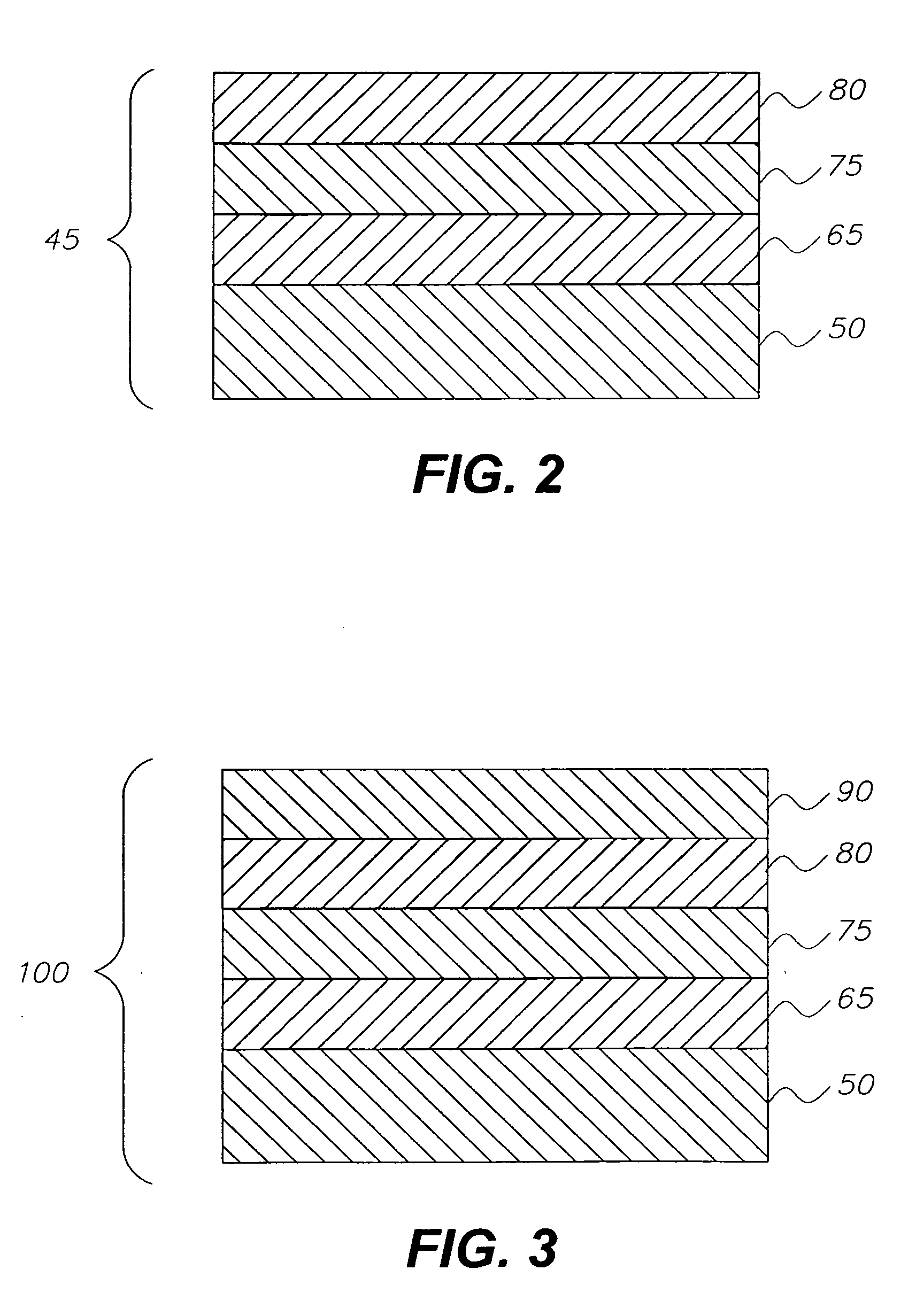
[0042] A donor element was constructed in the following manner: [0043] An antireflection layer of 40 nm of silicon and an absorption layer of 40 nm of chromium were vacuum-deposited in that order onto a 51 micron polyimide donor substrate. 20% of gold nanoparticles of size of 2-4 nm and 1-2% of IR absorbing dye were dispersed in 40 / 60 mixed solvent of ethanol / toluene and coated on the chrominum layer with a wet lay-down of 1 cc / sq ft. The sample was then dried at room temperature for 10 minutes to give a final thickness of about 300-500 nm.

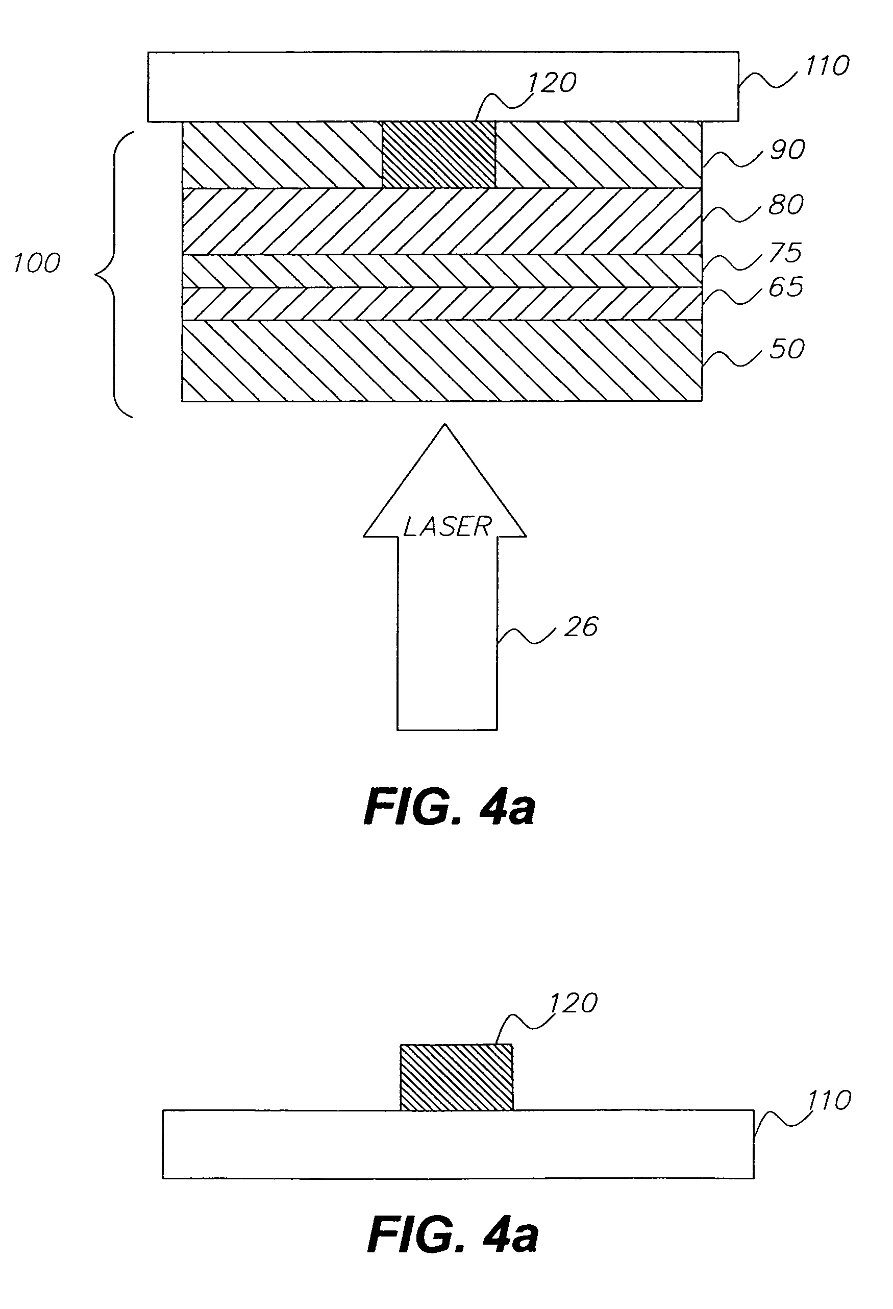
[0044] Receiving Substrate [0045] The receiving substrate used in the invention was 4 mil PET films with a 0.3 um of gelatin coating on the receiving side of the surface.

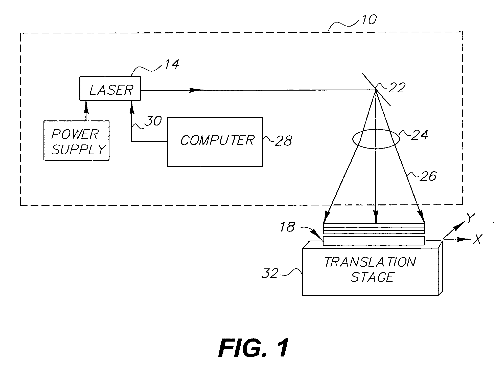
[0046] Annealed and Transferred of metal nanoparticle layer [0047] The metal nanoparticulate layer are placed in contact with the gel layer of the receiving substrate and held down by using the vacuum. In regions in which annealing and transferring is desired, a laser writer con...

example 2

[0048] A donor element and a receiving substrate satisfying the requirements of this invention was constructed as Example 1, except that 20% of silver nanoparticle with size of 50-70 nm (from CIMA Nanotech of St. Paul, Minn.) was dispersed in ethylene glycol butyl ether acetate solution containing 2% of IR absorbing dye.

example 3

[0049] A donor element and a receiving substrate satisfying the requirements of this invention was constructed as Example 1, except that 20% of silver nanoparticle size of 50-70 nm (from CIMA Nanotech of St. Paul, Minn.) was dispersed in water and ethanol mixed solvent containing 2% of IR absorbing dye.

[0050] The results of laser annealed and transferred patterned Au and Ag conductors on gel coated PET are shown in the Table 1.

TABLE 1Wet Lay-downDry ThicknessResistivity (Ohm-Coating Solution(cc / sq ft)(um)cm)Example 110.37.5 × 10−5Example 210.53.6 × 10−5Example 310.53.2 × 10−5

[0051] Table 1 shows that upon laser transferring and annealing, the resistivity transferred metal layers on the gel coated PET drops to a very conductive state. The nanoparticle layers not irradiated by the laser remain nonconductive on the donor substrates due to the lack of sintering.


PUM

PropertyMeasurementUnit
glass transition temperatureaaaaaaaaaa
sizesaaaaaaaaaa

Abstract

A method of forming a pattern of electrical conductors on a receiving substrate (110) comprises forming metal nanoparticles of a conductive material. A donor substrate (45) is formed. A layer of release material (75) is deposited on a first side of the donor substrate. The metal nanoparticles are deposited on the release material. The metal nanoparticulate layer are placed in contact with the receiving substrate. A pattern is written on a sandwich formed by the donor substrate and the receiving substrate, causing metal nanoparticles from the nanoparticulate layer (90) to anneal and transfer to the receiving substrate to form the pattern of electrical conductors on the receiving substrate.

Description

CROSS REFERENCE TO RELATED APPLICATIONS [0001] Reference is made to commonly-assigned copending U.S. patent application Ser. No. 10 / 881,301, filed Jun. 30, 2004, entitled FORMING ELECTRICAL CONDUCTORS ON A SUBSTRATE, by Yang et al.; the disclosure of which is incorporated herein.FIELD OF THE INVENTION [0002] The invention relates in general to forming a pattern of conductors on a receiving substrate and in particular to forming conductors on a receiving substrate by annealing and transferring metal nanoparticles from a donor substrate to a receiving substrate. BACKGROUND OF THE INVENTION [0003] It is often necessary to print large area electrical circuits with conductors having at least one lateral dimension of 1-1000 microns. One process for accomplishing this type of circuit printing is using vacuum deposition. This method, however, is a high-cost operation and is only suitable for batch processing. [0004] Another method of constructing electrical circuits is inkjet printing of pa...

Claims


Application Information

Patent Timeline
Patent Type & Authority Applications(United States)
IPC IPC(8): G03C5/00
CPCH05K3/046H05K2201/0112H05K2203/107H05K2203/0528H05K2201/0257B82Y30/00H05K3/00
Inventor NGUYEN, KELVINYANG, ZHIHAO
Owner EASTMAN KODAK CO
Why Eureka
Try Eureka