

Thin film forming device and thin film forming method
- Summary
- Abstract
- Description
- Claims
- Application Information
AI Technical Summary
Benefits of technology
Problems solved by technology
Method used
Image

Examples
Embodiment Construction
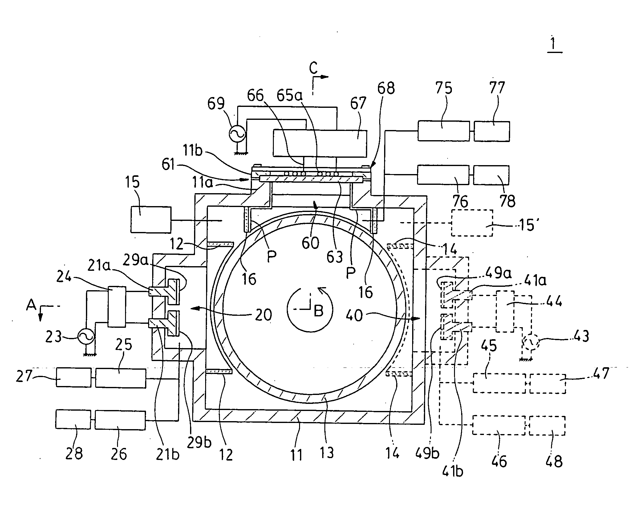
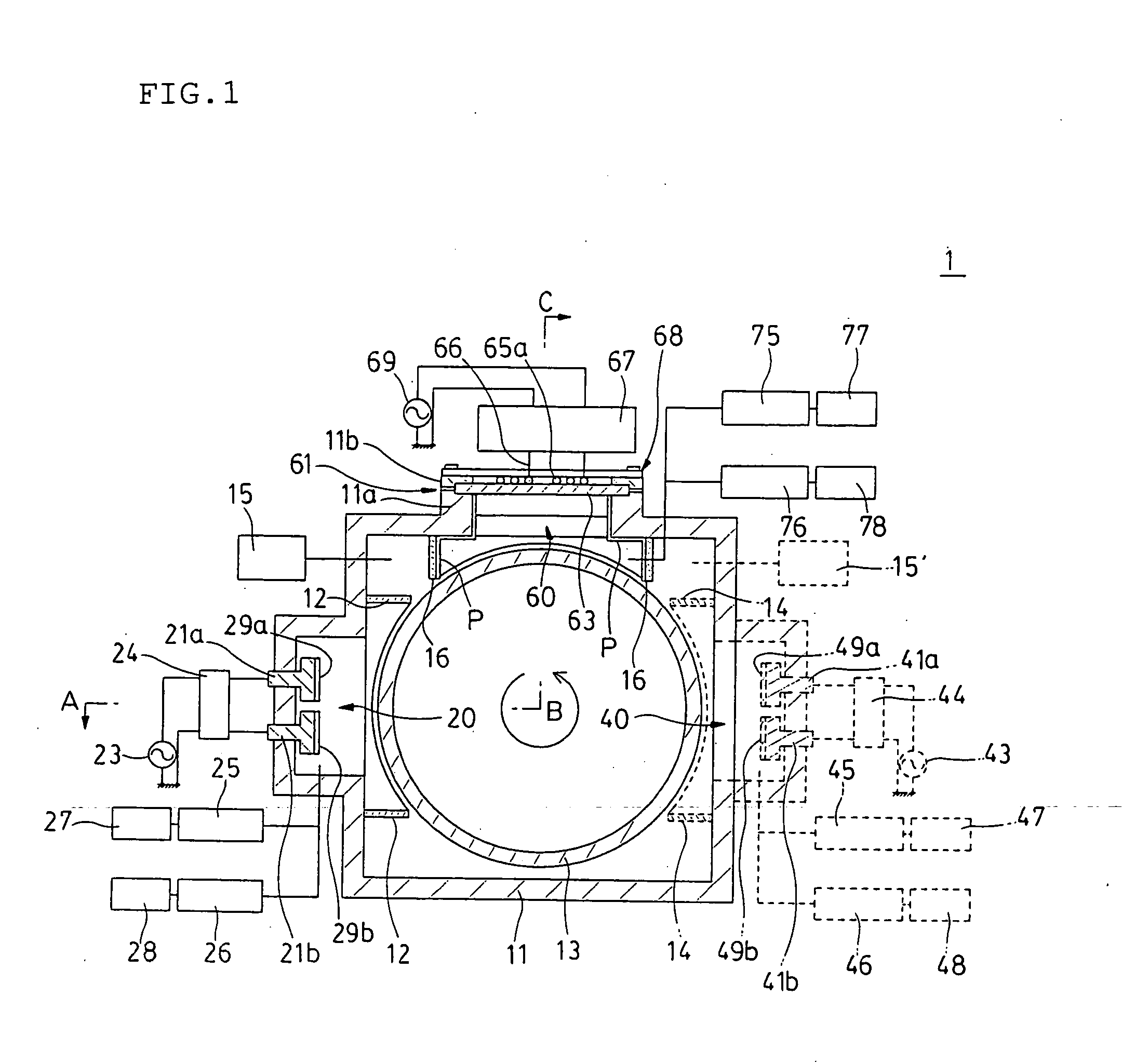
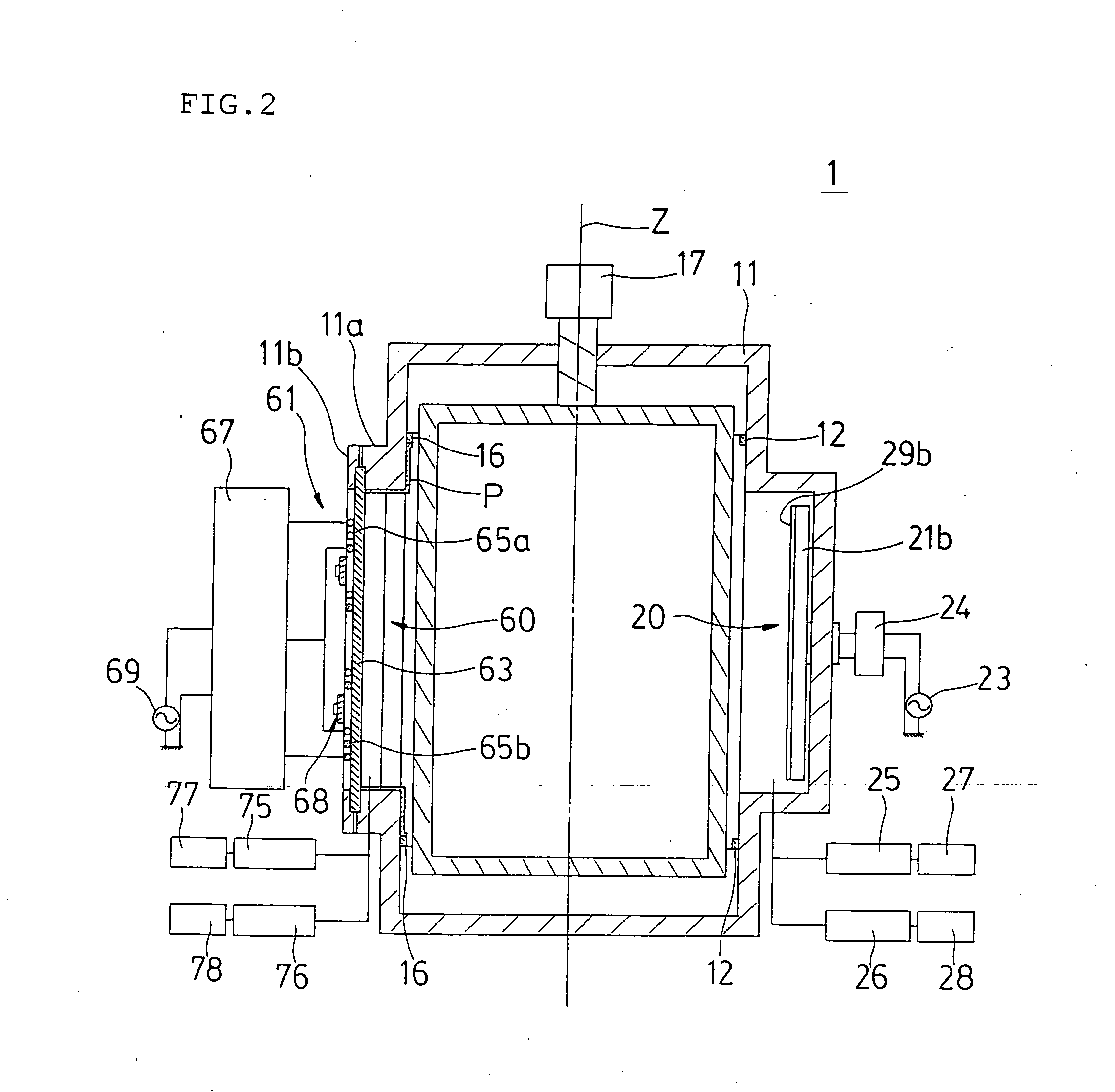
[0045] An embodiment of the present invention will next be described in detail with reference to the drawings. Members, arrangement, and the like to be described below should not be construed as limiting the invention, but may be modified in various forms without departing from the scope of the invention.
[0046]FIGS. 1 and 2 are explanatory views for explaining a sputtering apparatus 1. FIG. 1 is an explanatory top view with a partial section provided for easy understanding. FIG. 2 is a partially sectional, explanatory side view taken along line A-B-C of FIG. 1. The sputtering apparatus 1 is an example of a thin film deposition apparatus of the present invention.
[0047] The sputtering apparatus 1 of the present embodiment performs magnetron sputtering, which is a type of sputtering. However, the type of sputtering is not limited thereto. The sputtering apparatus 1 may perform another known type of sputtering, such as diode sputtering without use of magnetron discharge.
[0048] The sp...
PUM
| Property | Measurement | Unit |
|---|---|---|
| Plasma power | aaaaa | aaaaa |
Abstract
Description
Claims
Application Information