Semiconductor device and method of manufacturing the same

a technology of semiconductor devices and capacitors, applied in the direction of semiconductor devices, basic electric elements, electrical equipment, etc., can solve the problem of a relatively high voltage in the memory, and achieve the effect of widening the voltage of the applied voltage to the capacitor

Inactive Publication Date: 2006-12-14
FUJITSU SEMICON LTD
View PDF11 Cites 17 Cited by
  • Summary
  • Abstract
  • Description
  • Claims
  • Application Information

AI Technical Summary

Benefits of technology

[0020] In addition, contact between the resist pattern and the upper electrode is prevented by the auxiliary mask. Therefore, the upper surface of the upper electrode does not become rough even when the upper electrode is exposed to the oxygen-containing atmosphere such as the recovery annealing applied to the capacitor dielectric film.
[0023] Further, the step of etching the second conductive film may be performed by using an ICP (Inductively Coupled Plasma) etching equipment in which the quartz is employed as at least a part of a chamber. If doing so, a minute quantity of oxygen is supplied from the quartz, which is attacked by the plasma, into the etching atmosphere. Since the oxygen acts to oxidize a surface of the auxiliary mask and decelerate the etching rate of the auxiliary mask, it can be prevented that the thin auxiliary mask disappears owing to the above etching.
[0024] In the case where the gas mixture consisting of the halogen gas and the inert gas is used as the etching gas, such reduction in the etching rate of the auxiliary mask can be attained effectively when an occupation rate of the inert gas in the etching gas is set to 60% or more in terms of flow rate ratio.
[0030] According to the present invention, the upper surface of the upper electrode is planarized, and the thin thickness portion having a thin thickness is not formed in the upper electrode. Therefore, the entering of the reducing substance such as the hydrogen, or the like into the capacitor dielectric film constituting the capacitor can be blocked easily by the upper electrode.
[0031] In addition, a sectional shape of the upper electrode can be stabilized because the thin thickness portion is not formed. Therefore, it can be suppressed that electric characteristics of the capacitor, such as the electrostatic capacity, are varied every cell, and a margin of the applied voltage to the capacitor can be widened.

Problems solved by technology

However, the flash memory has such a disadvantage that the memory needs a relatively high voltage because a tunnel current must be supplied to the gate insulating film in writing or erasing the information.

Method used


Image

  • Semiconductor device and method of manufacturing the same
  • Semiconductor device and method of manufacturing the same
  • Semiconductor device and method of manufacturing the same

Examples


Embodiment Construction

[0037] (1) Preliminary Explanation

[0038] Prior to an embodiment of the present invention, preliminary matters of the present invention will be explained hereunder.

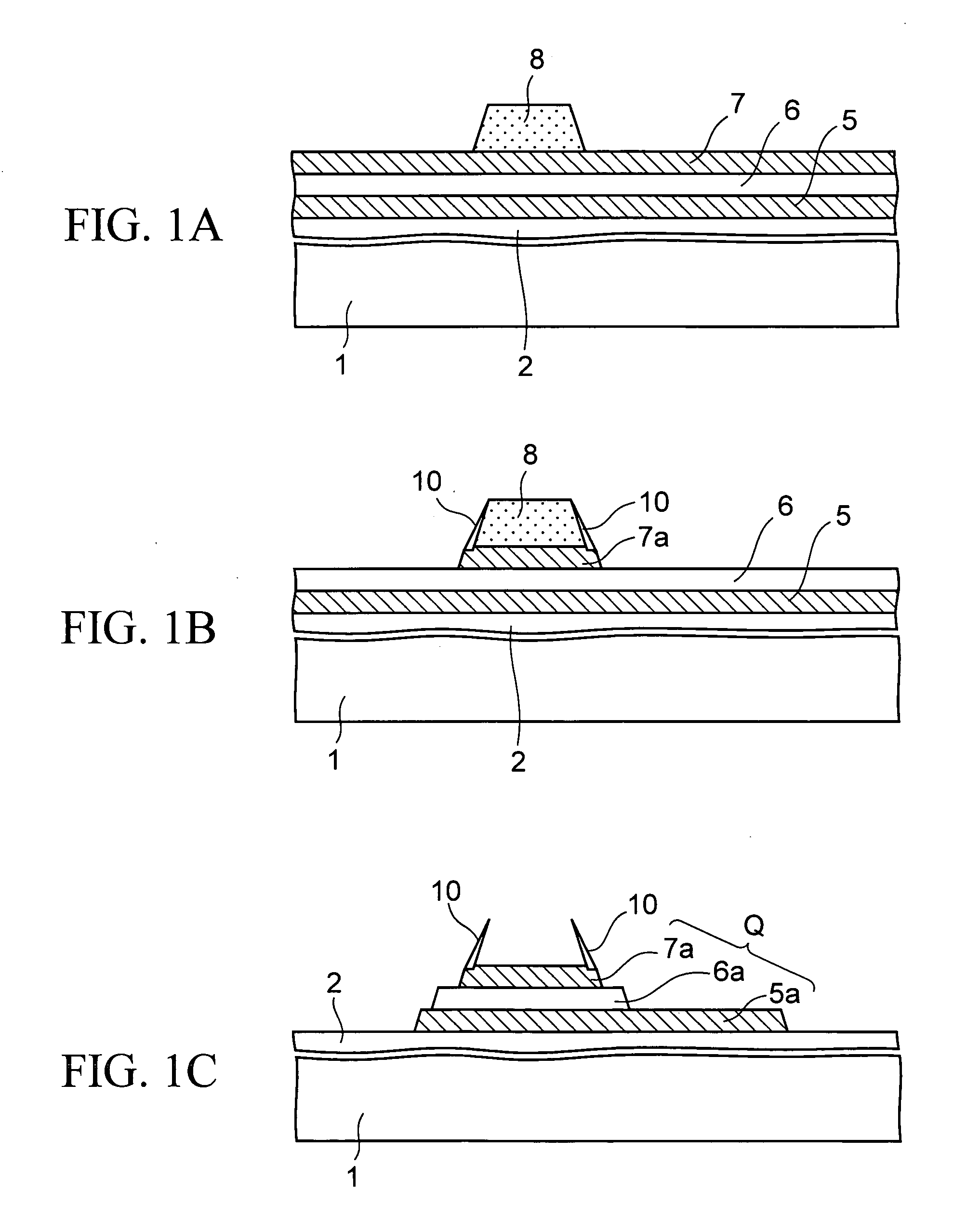
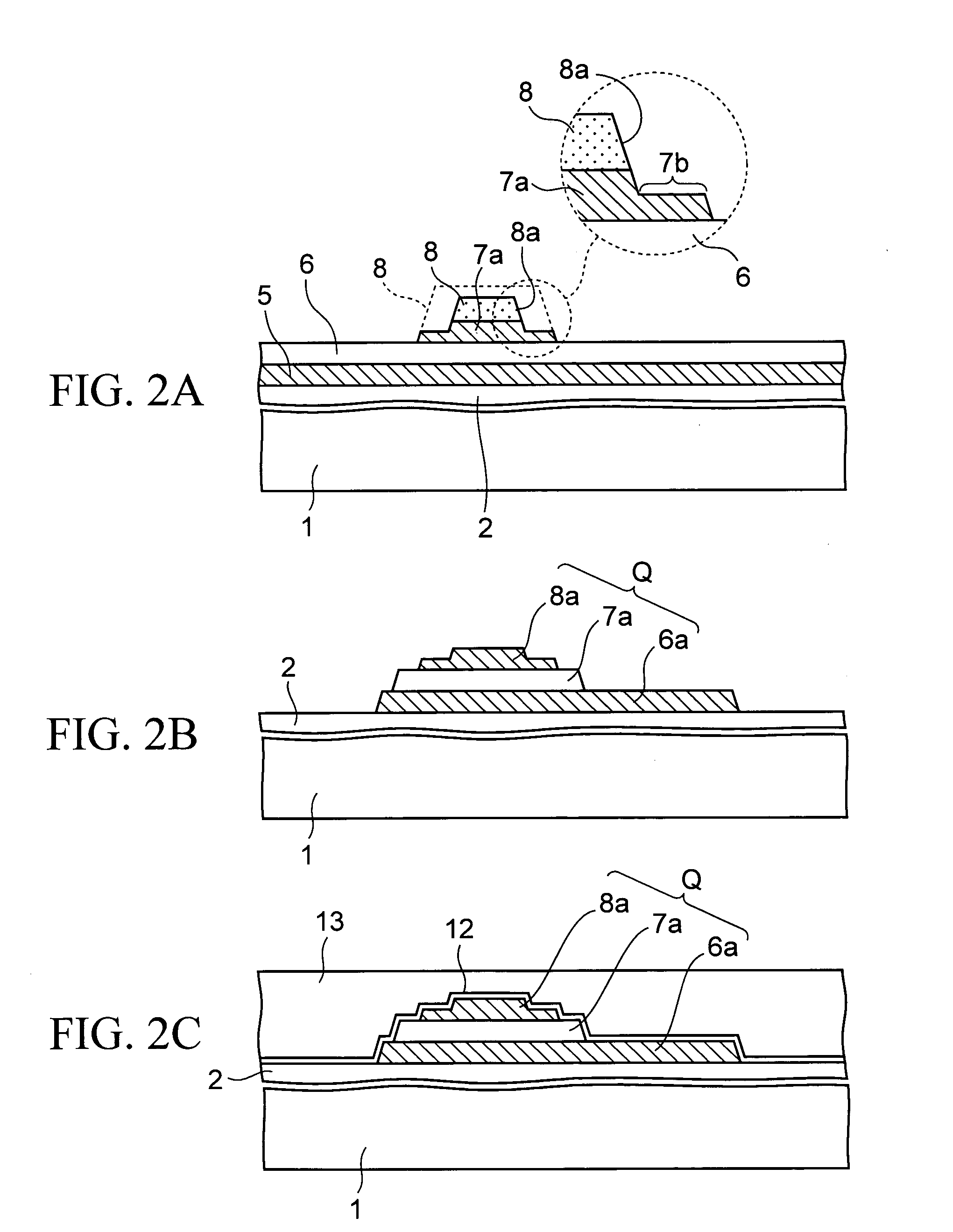
[0039]FIGS. 1A to 1C are sectional views of a virtual FeRAM in the middle of manufacture.

[0040] At first, as shown in FIG. 1A, an underlying insulating film 2 is formed over a silicon substrate 1. Then, a first conductive film 5, a ferroelectric film 6, and a second conductive film 7 are formed in this order on the underlying insulating film 2. Then, a photoresist is coated on the second conductive film 7, and then a resist pattern 8 having a profile of the capacitor upper electrode is formed by exposing / developing the photoresist. Here, typically a noble metal film such as an iridium (Ir) film, a platinum (Pt) film, or the like, or a noble metal oxide film such as an iridium oxide (IrOx) film, or the like is employed as the second conductive film 7. Also, a PZT (Lead Zirconate Titanate) film is employed as the ferroele...


PUM

PropertyMeasurementUnit
thicknessaaaaaaaaaa
thicknessaaaaaaaaaa
thicknessaaaaaaaaaa

Abstract

A semiconductor device manufacturing method, includes a step of forming a first alumina film (underlying insulating film) 37 on a semiconductor substrate 20, a step of forming a first conductive film 41, a ferroelectric film 42, and a second conductive film 43 in sequence on the first alumina film 37, a step of forming a mask material film 45 on the second conductive film 43, a step of shaping the mask material film 45 into an auxiliary mask 45a, a step of shaping the second conductive film 43 into an upper electrode 43a by an etching using the auxiliary mask 45a and a first resist pattern 46 as a mask, a step of shaping the ferroelectric film 42 into a capacitor dielectric film 42a by patterning, and a step of shaping the first conductive film 41 into a lower electrode 41a by patterning, whereby a capacitor Q is constructed by the lower electrode 41, the capacitor dielectric film 42a, and the upper electrode 43a.

Description

CROSS-REFERENCE TO RELATED APPLICATIONS [0001] This application is based on and claims priority of Japanese Patent Application No. 2005-169377 filed on Jun. 9, 2005, the entire contents of which are incorporated herein by reference. BACKGROUND OF THE INVENTION [0002] 1. Field of the Invention [0003] The present invention relates to a semiconductor device and a method of manufacturing the same. [0004] 2. Description of the Related Art [0005] As the nonvolatile memory capable of storing information even after the power supply is turned off, the flash memory and the ferroelectric memory are known. [0006] Out of them, the flash memory has a floating gate buried in a gate insulating film of an insulated-gate field effect transistor (IGFET), and stores the information by accumulating electric charges representing the stored information in this floating gate. However, the flash memory has such a disadvantage that the memory needs a relatively high voltage because a tunnel current must be s...

Claims


Application Information

Patent Timeline
Patent Type & Authority Applications(United States)
IPC IPC(8): H01L21/311H01L29/40
CPCH01L21/02071H01L21/32134H01L27/11507H01L21/32139H01L27/11502H01L21/32136Y10S438/95H10B53/30H10B53/00
Inventor KOMURO, GENICHIKIUCHI, KENJI
Owner FUJITSU SEMICON LTD
Why Eureka
Try Eureka