
Semiconductor device and manufacturing method of the semiconductor device

a semiconductor and manufacturing method technology, applied in the direction of semiconductor devices, basic electric elements, electrical appliances, etc., can solve the problems of junction leakage, difficult to contribute to the reduction of resistance of the source/drain layer sufficiently, and increase the current in an off-state field-effect transistor. , to achieve the effect of suppressing the short channel effect and reducing the resistance of the source/drain layer

Inactive Publication Date: 2006-12-21
SEIKO EPSON CORP +1
View PDF4 Cites 39 Cited by
  • Summary
  • Abstract
  • Description
  • Claims
  • Application Information

AI Technical Summary

Benefits of technology

[0010] It is an object of the present invention to provide a semiconductor device in which while junction leakage is suppressed, resistance of a source / drain layer is reduced, and a short channel effect can be suppressed, and a manufacturing method of the semiconductor device.

Problems solved by technology

Therefore, in the field-effect transistor in which the gate length is reduced to about 100 nm or less, it becomes difficult to suppress a short channel effect sufficiently, thus causing the problem that a leakage current in an off state of the field-effect transistor increases.
Further, in the method of siliciding the surfaces of the source / drain layer, when the silicide layer reaches the joint surfaces of the source / drain layer and the channel region, junction leakage is caused, and therefore, it is necessary to make the silicide layer thin, thus causing the problem of making it difficult to contribute to reduction in resistance of the source / drain layer sufficiently.
In the method disclosed in Patent Document 1, there is the problem that when the silicide layer reaches the area in the vicinity of the joint surfaces of the source / drain layer and the channel region, and when the silicide reaction proceeds beyond the joint surfaces of the source / drain layer and the channel region, junction leakage is caused.

Method used


Image

  • Semiconductor device and manufacturing method of the semiconductor device
  • Semiconductor device and manufacturing method of the semiconductor device
  • Semiconductor device and manufacturing method of the semiconductor device

Examples


first embodiment

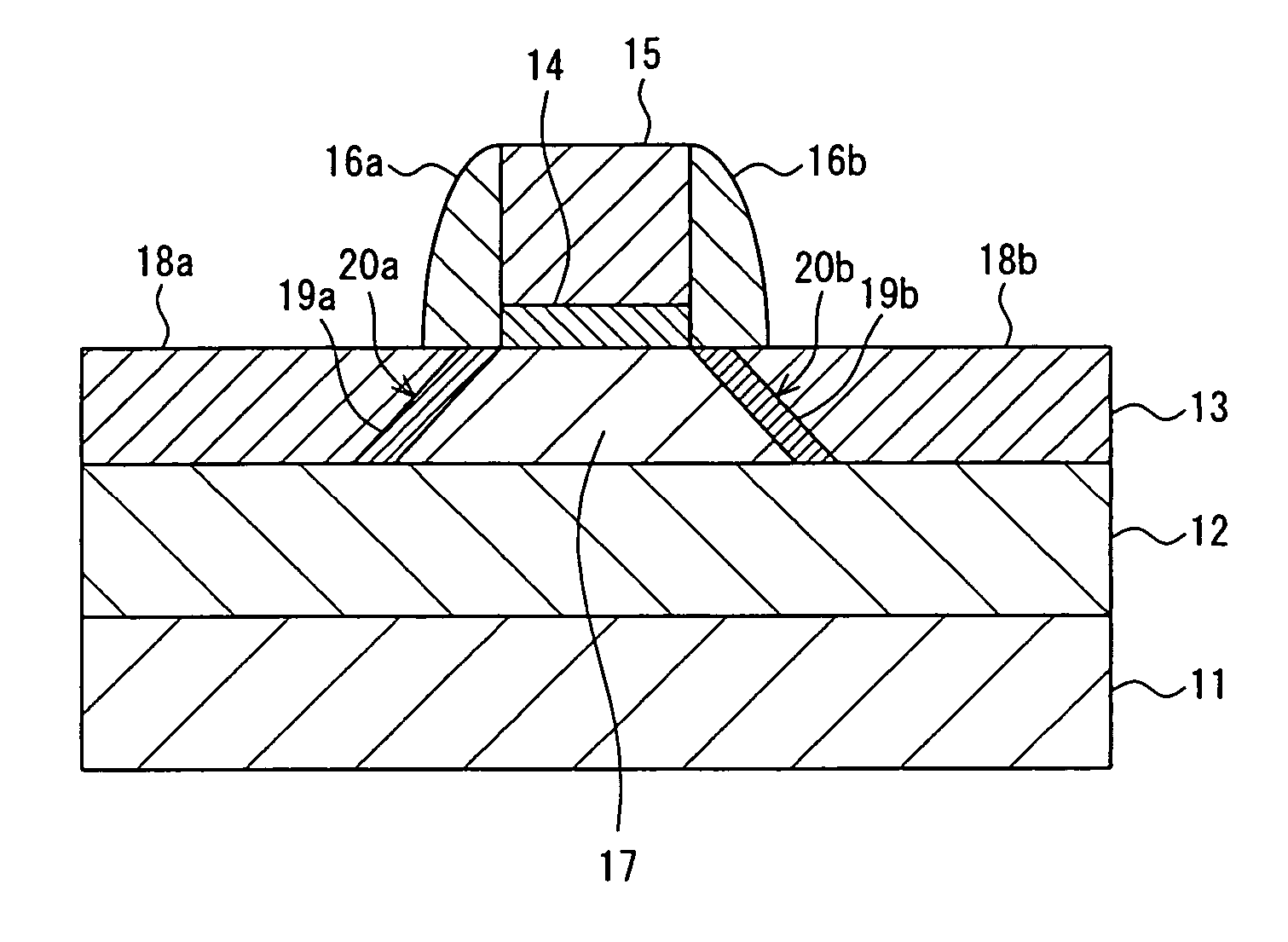
[0045]FIG. 1 is a sectional view showing a schematic construction of a semiconductor device according to the present invention.

[0046] In FIG. 1, an insulating layer 12 is formed on a supporting substrate 11, and a monocrystal semiconductor layer 13 is formed on the insulating layer 12. As the supporting substrate 11, a semiconductor substrate of Si, Ge, SiGe, GaAs, InP, GaP, GaN, SiC or the like may be used, or an insulating substrate of glass, sapphire, ceramics or the like may be used. As the material of the monocrystal semiconductor layer 13, for example, Si, Ge, SiGe, SiC, SiSn, PbS, GaAs, InP, GaP, GaN, ZnSe or the like can be used, and as the insulating layer 12, an insulating layer or a buried insulating film of, for example, SiO2, SiON, Si3N4 or the like can be used. As the semiconductor substrate with the monocrystal semiconductor layer 13 formed on the insulating layer 12, for example, an SOI substrate can be used, and as the SOI substrate, an SIMOX (Separation by Implante...

second embodiment

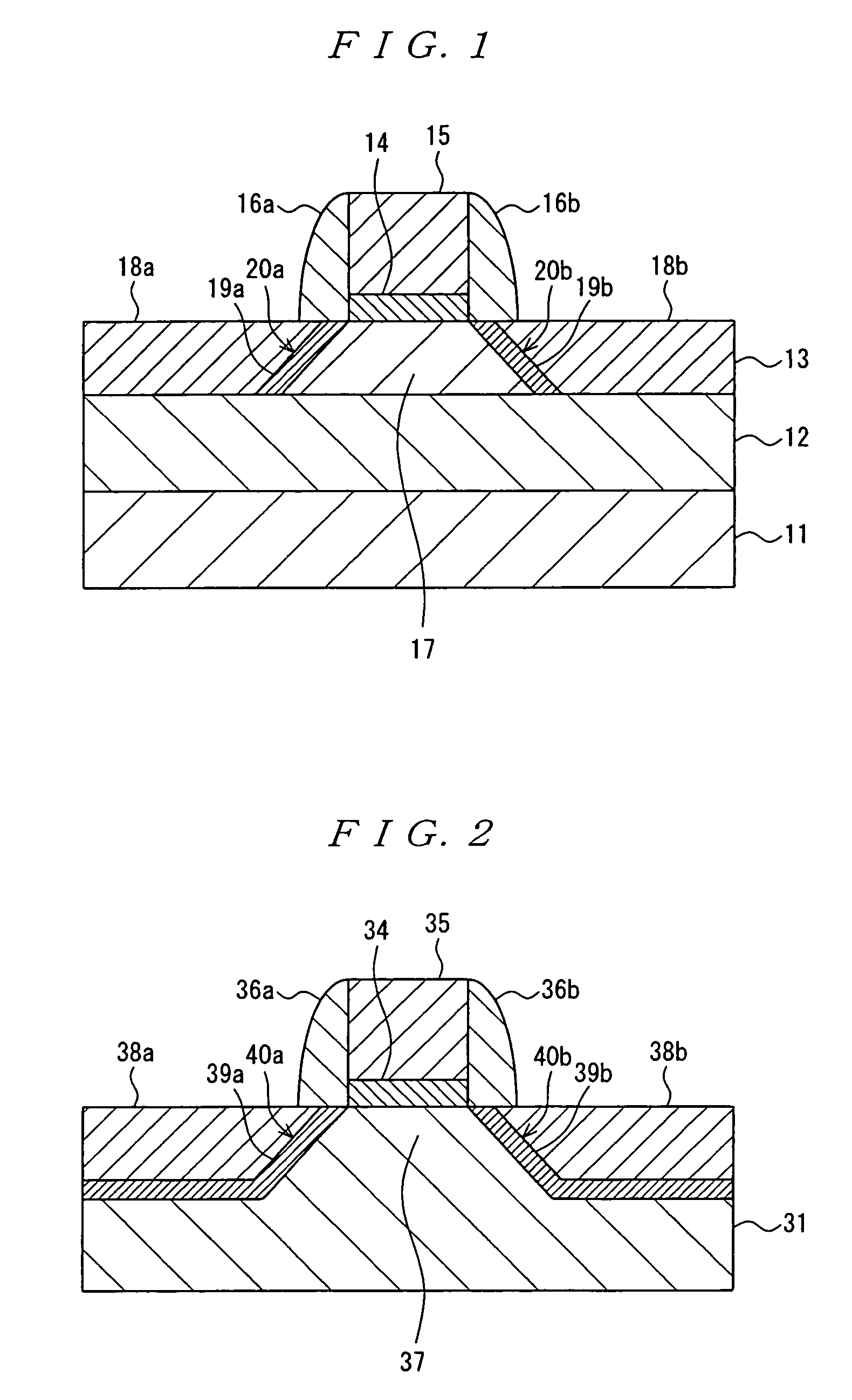
[0052]FIG. 2 is a sectional view showing a schematic construction of a semiconductor device according to the present invention.

[0053] In FIG. 2, a gate electrode 35 is disposed on a semiconductor substrate 31 via a gate insulating film 34. A side wall 36a is formed at one side wall of the gate electrode 35, and a side wall 36b is formed at the other side wall of the gate electrode 35. A source layer 38a composed of an alloy layer buried in the semiconductor substrate 31 is disposed at one side of the gate electrode 35. Here, in the alloy layer composing the source layer 38a, a joint surface to a channel region 37 is formed along a crystal orientation face 40a of the semiconductor substrate 31. A drain layer 38b composed of an alloy layer buried in the semiconductor substrate 31 is disposed at the other side of the gate electrode 35. Here, in the alloy layer composing the drain layer 38b, a joint surface to the channel region 37 is formed along a crystal orientation face 20b of the s...

third embodiment

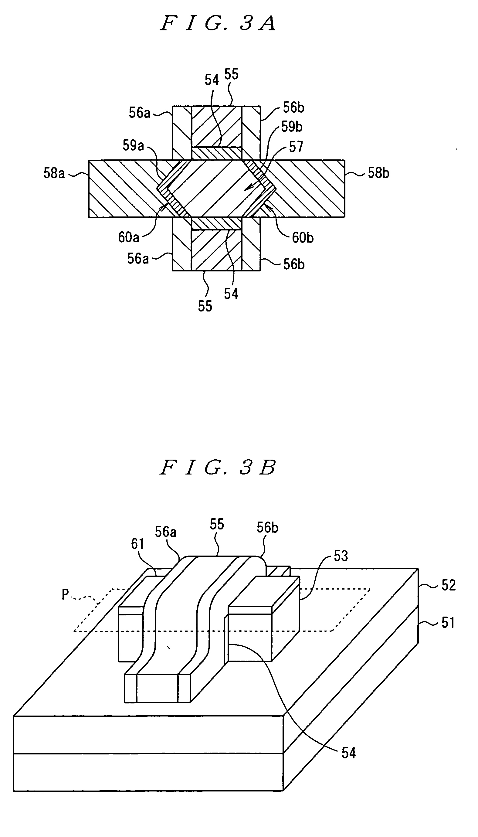
[0056]FIG. 3B is a perspective view showing a schematic construction of a semiconductor device according to the present invention, and FIG. 3A is a sectional view which is cut along a P plane in FIG. 3B.

[0057] In FIGS. 3A and 3B, an insulating layer 52 is formed on a supporting substrate 51, and a monocrystal semiconductor layer 53 having a fin shape is formed on the insulating layer 52. An insulating layer 61 is formed on the monocrystal semiconductor layer 53, and at side walls at both sides of the monocrystal semiconductor layer 53, a gate electrode 55 disposed to stride over the monocrystal semiconductor layer 53 is formed via a gate insulating film 54. A side wall 56a is formed at one side wall of the gate electrode 55, and a side wall 56b is formed at the other side wall of the gate electrode 55. At one side of the gate electrode 55, a source layer 58a in which the entire monocrystal semiconductor layer 53 is filled with an alloy layer is disposed. Here, in the alloy layer com...


PUM


Abstract

A semiconductor device includes a semiconductor layer formed on an insulating layer; a gate electrode disposed on said semiconductor layer via a gate insulating film; a source / drain layer composed by including an alloy layer or a metal layer with a bottom surface in contact with the insulating layer, with joint surfaces to a channel region disposed along crystal orientation faces of said semiconductor layer; and impurity-doped layers formed in a self-aligned manner along interfaces of the alloy layer or the metal layer, and said semiconductor layer.

Description

[0001] The entire disclosure of Japanese Patent Application No. 2005-169631, filed Jun. 9, 2005, is expressly incorporated by reference herein. BACKGROUND [0002] 1. Field of the Invention [0003] The present invention relates to a semiconductor device and a manufacturing method of the semiconductor device, and particularly is preferable for application in a field-effect transistor reduced to a submicron order or less. [0004] 2. Description of the Related Art [0005] In the field-effect transistors of recent years, gate lengths are shortened to a submicron order to promote densification and speedup of semiconductor integrated circuits. In order to suppress increase in resistance of source / drain layers of miniaturized field-effect transistors, silicidation of surfaces of the source / drain layers is performed. [0006] For example, JP-A-2002-110991 (hereinafter referred to as Patent Document 1) discloses a method for forming a joint interface of a diffusion layer which is a silicon portion ...

Claims


Application Information

Patent Timeline
IPC IPC(8): H01L29/78
CPCH01L21/2257H01L29/04H01L29/41733H01L29/41766H01L29/41775H01L29/78609H01L29/66545H01L29/66575H01L29/66636H01L29/66772H01L29/785H01L29/41783
Inventor WATANABE, YUKIMUNEMIGITA, SHINJIMISE, NOBUYUKI
Owner SEIKO EPSON CORP
Features
  • Generate Ideas
  • Intellectual Property
  • Life Sciences
  • Materials
  • Tech Scout
  • Unparalleled Data Quality
  • Higher Quality Content
  • 60% Fewer Hallucinations
Learn More