Semiconductor device and method of manufacturing the same

a technology of semiconductors and semiconductors, applied in the direction of semiconductor devices, basic electric elements, electrical equipment, etc., can solve the problems of spoiled pti element isolation function, extremely low energy, and become a problem, so as to reduce the leakage current by the junction capacitance of source and drain regions, and reduce the leakage current. the effect of low energy

Inactive Publication Date: 2006-12-28
RENESAS TECH CORP
View PDF3 Cites 10 Cited by
  • Summary
  • Abstract
  • Description
  • Claims
  • Application Information

AI Technical Summary

Benefits of technology

[0019] According to the semiconductor device concerning the present invention, since source drain regions include the first and the second impurity ions with which mass numbers differ mutually, the source and drain regions come to have an impurity concentration profile gradual and at high concentration, and a deep profile. That is, impurity concentration in the depth of a boundary face with a silicide layer in the source and drain regions can be made high, and the distance of the pn junction surface of the source and drain region bottom and the silicide layer can be detached. Therefore, resistance reduction between silicide layer-source and drain regions can be aimed at, and it is possible to reduce the leakage current by the junction capacitance of the source and drain regions.
[0020] According to the manufacturing method of the semiconductor device concerning the present invention, since the concentration of the first impurity ion becomes more than the concentration of the second impurity ion in the boundary face of a suicide layer and source and drain regions after a heat treatment, the impurity concentration of the boundary face concerned becomes high and resistance reduction between suicide layer-source and drain regions can be aimed at. Since the first and the second impurity ions are implanted in an order of a small mass number, the first impurity ion can be more deeply implanted with low energy by channeling. Therefore, since the source and drain regions can be formed by a deep profile, the distance of the pn junction surface of the source and drain region bottom and the silicide layer can be detached, and the leakage current by the junction capacitance of the source and drain regions can be reduced.

Problems solved by technology

When impurity ion penetrates through PTI and an impurity layer of the same conductivity type as the source and drain regions is formed in the SOI layer under PTI, the element isolation function of PTI will be spoiled and it will become a problem.
Therefore, when PTI is thin, it is necessary to perform impurity ion implantation for source and drain region formation with extremely low energy.

Method used


Image

  • Semiconductor device and method of manufacturing the same
  • Semiconductor device and method of manufacturing the same
  • Semiconductor device and method of manufacturing the same

Examples


embodiment 1

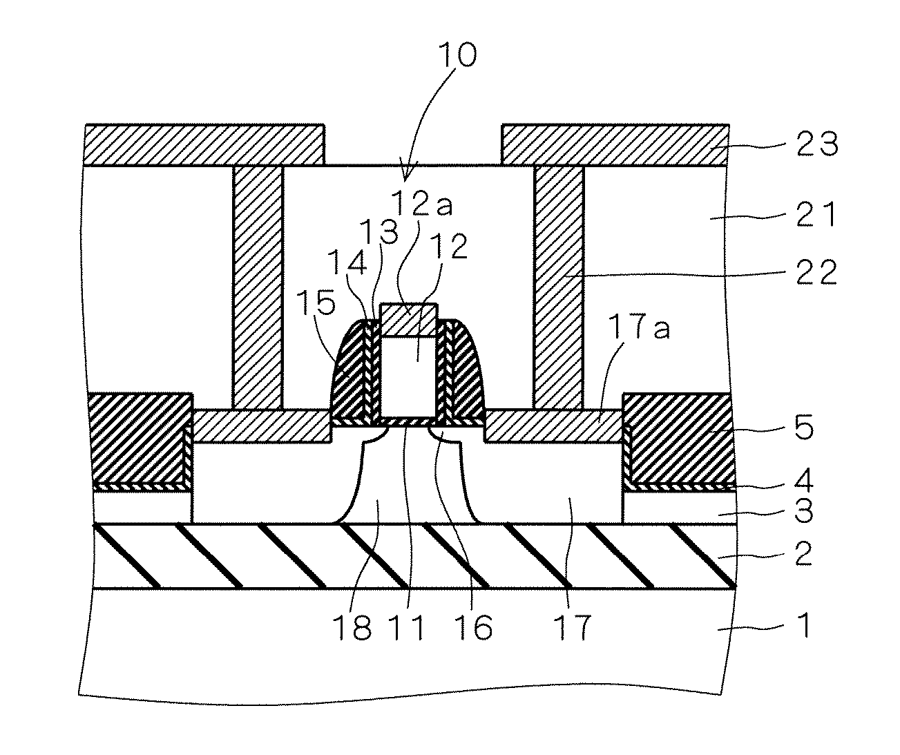
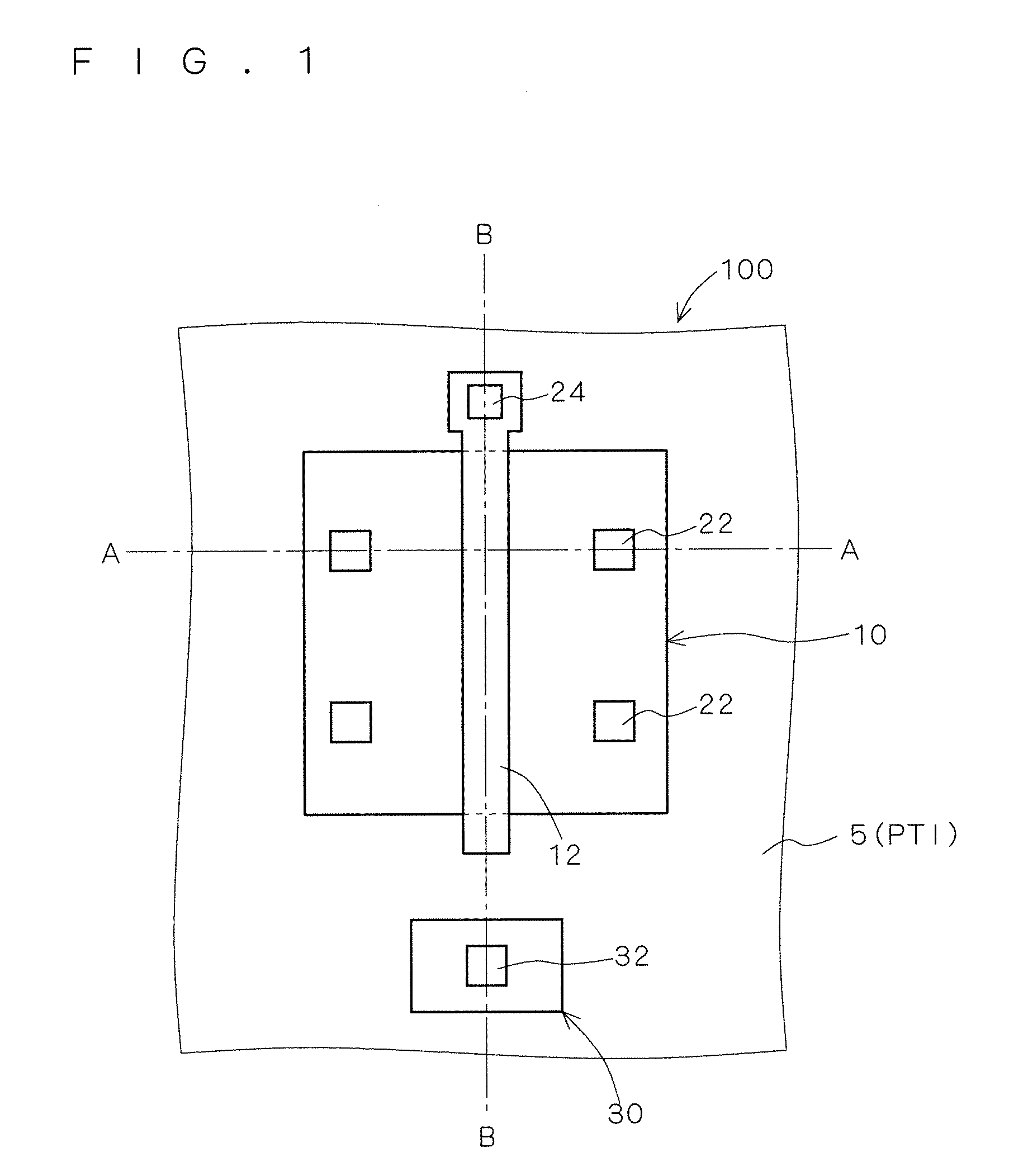
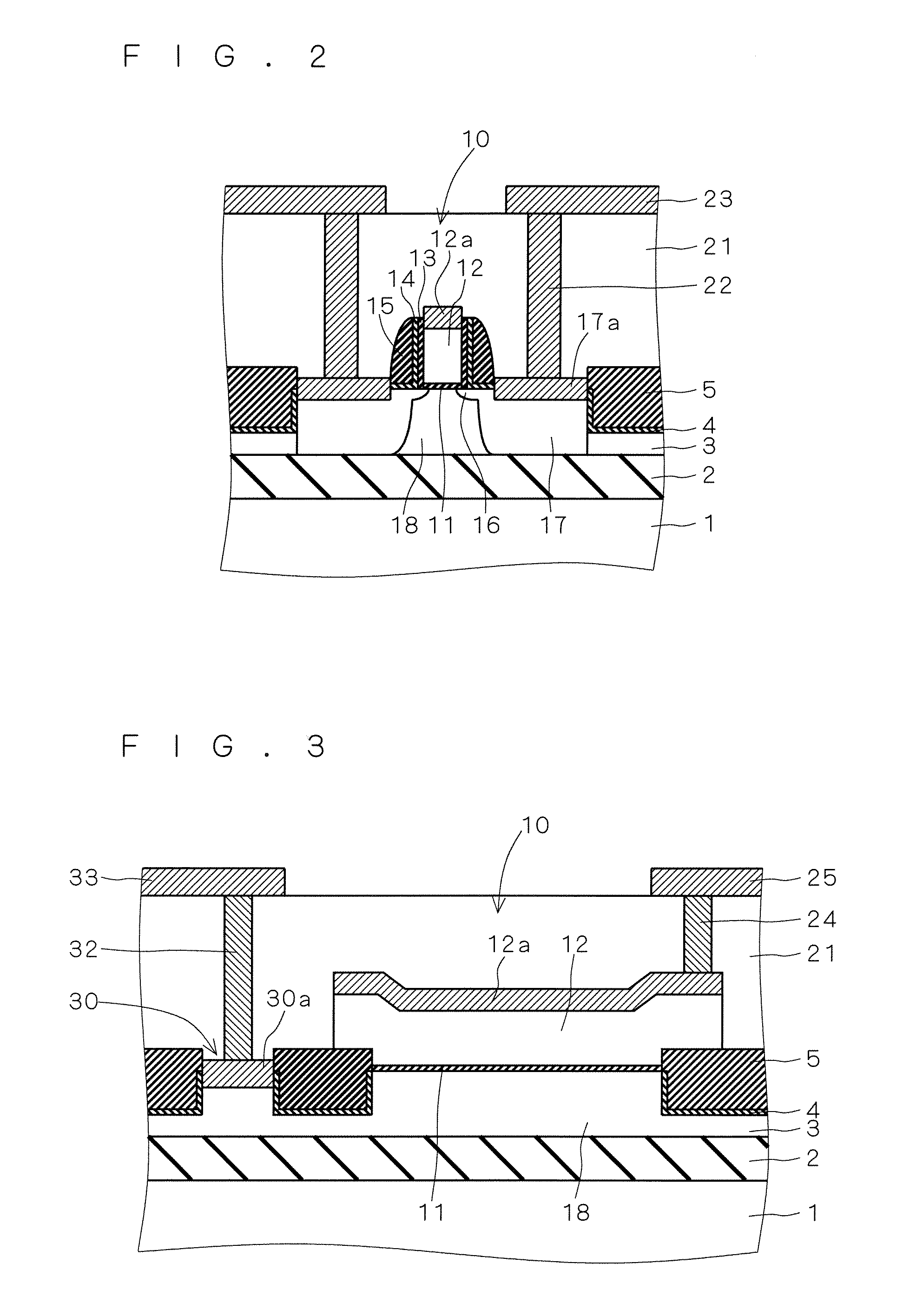
[0032]FIG. 1-FIG. 3 are the drawings showing the structure of the semiconductor device concerning Embodiment 1 of the present invention. FIG. 1 is a top view of the MOS transistor with which the semiconductor device concerned is provided, and FIG. 2 and FIG. 3 are the cross-sectional views which are taken along the A-A line and the B-B line of FIG. 1, respectively. Through these drawings, the same reference is given to the same element.

[0033] The semiconductor device concerning this embodiment has MOS transistor 10, and cell 30 for body electric-potential fixation which is a terminal (body terminal) for setting up the body electric potential on SOI substrate 100 like FIG. 1. Here, on the convenience of explanation, the explanation is made, assuming that MOS transistor 10 is an n channel type transistor (nMOS transistor). However, although also mentioning later, the present invention is applicable also to a p channel type transistor (pMOS transistor).

[0034] With reference to FIG. 2...

embodiment 2

[0069] In order to prevent degradation of the isolation characteristics, it is necessary to make the impurity ion implanted in the case of source and drain region 17 formation not penetrate through isolation insulating layer 5, when PTI is adopted as isolation insulating layer 5, as stated previously. In order to suppress this penetration, it is possible to thicken isolation insulating layer 5, but since SOI layer 3 under the isolation insulating layer 5 concerned needs to secure moderate thickness, there is a limitation in forming isolation insulating layer 5 deeply. Then, it is possible to make high the height (height h shown in FIG. 10) of the portion to which isolation insulating layer 5 projects from the substrate. However, since it is necessary to prevent that the residual substance of polysilicon remains in the case of patterning of gate electrode 12 into the level difference portion of SOI layer 3 and isolation insulating layer 5, there is a limitation also in it.

[0070] Thu...

embodiment 3

[0079] In above-mentioned Embodiment 2, substantial thickness of isolation insulating layer 5 in the ion-implantation step for source and drain region 17 formation was thickened by using silicon oxide film 114 used as sidewall oxide film 14.

[0080] In Embodiment 3, spacer oxide film 13 and sidewall oxide film 14 are formed like Embodiment 1. That is, the forming portions of the source and drain regions 17 concerned in SOI layer 3 are exposed in the case of formation of spacer oxide film 13 and sidewall oxide film 14. And after that, silicon oxide film 60 is separately deposited on the whole surface like FIG. 21, and the ion implantation for source and drain region 17 formation is performed through the silicon oxide film 60 concerned. That is, in the case of the ion implantation for source and drain region 17 formation, silicon oxide film 60 is formed on the upper surface of isolation insulating layer 5.

[0081] That is, the thickness of isolation insulating layer 5 in the ion-implant...


PUM


Abstract

In the semiconductor device which has partial trench isolation as isolation between elements formed in an SOI substrate, resistance reduction of the source drain of a transistor and reduction of leakage current are aimed at. A MOS transistor is formed in the active region specified by the isolation insulating layer in the SOI layer formed on the buried oxide film layer (BOX layer). An isolation insulating layer is a partial trench isolation which has not reached a BOX layer, and source and drain regions include the first and the second impurity ion which differs in a mass number mutually.

Description

CROSS-REFERENCE TO RELATED APPLICATION [0001] The present application claims priority from Japanese patent application No. 2005-184295 filed on Jun. 24, 2005, the content of which is hereby incorporated by reference into this application. FIELD OF THE INVENTION [0002] The present invention relates to a semiconductor device which has SOI (Silicon-On-Insulator) structure, and its manufacturing method. DESCRIPTION OF THE BACKGROUND ART [0003] The SOI device using an SOI substrate which stacks a supporting substrate, an insulator layer, and a silicon layer (SOI layer) in layers attracts attention as a device which can improve the performance of a semiconductor device in recent years. For example, a MOS (Metal-Oxide Semiconductor) transistor formed in the SOI substrate has the small parasitic capacitance of the source and drain regions, and operation of a high speed and low power is possible for it. [0004] Improvement in performance of a MOS transistor formed in a silicon substrate of a ...

Claims


Application Information

Patent Timeline
Patent Type & Authority Applications(United States)
IPC IPC(8): H01L29/76
CPCH01L21/76283H01L21/84H01L29/78609H01L29/458H01L29/66772H01L27/1203
Inventor TSUJIUCHI, MIKIOIWAMATSU, TOSHIAKIIPPOSHI, TAKASHI
Owner RENESAS TECH CORP
Why Eureka
Try Eureka