Replacement gate field effect transistor with germanium or SiGe channel and manufacturing method for same using gas-cluster ion irradiation

a field effect transistor and germanium channel technology, applied in the direction of electrical equipment, semiconductor devices, electrical discharge tubes, etc., can solve the problems of reducing device speed performance, high cost, and disadvantages of high-k gate dielectric with metal gate, and achieves minimal diffusion and improved carrier mobility.

Inactive Publication Date: 2006-12-28
TEL EPION
View PDF7 Cites 61 Cited by
  • Summary
  • Abstract
  • Description
  • Claims
  • Application Information

AI Technical Summary

Benefits of technology

[0011] By providing a germanium or SiGe channel in a p-channel MISFET or n-channel MISFET, carrier mobility is improved. A germanium or SiGe channel can be formed in a FET formed on a silicon or silicon-on-insulator substrate by using selective Ge infusion by energetic gas cluster ion beam irradiation. This can be achieved using a “replacement” gate process flow and masking step where the Ge or SiGe channel is formed after source-drain extension formation and after source-drain formation. The Ge is infused through the replacement gate mask prior to high-k gate dielectric deposition and gate formation. The infused Ge or SiGe channel may be doped with p-type or n-type dopants and may be activated and annealed at low temperatures with minimal diffusion. The infused Ge is limited to only the channel region and not the source-drain extension regions nor the deep source-drain regions. After gas-cluster ion beam Ge infusion, the high-k gate dielectric gate insulator film is deposited, followed by fabrication of a gate electrode. Infusion of Ge into Si to form Ge and / or SiGe films by GCIB irradiation is a subject of US Patent Application publication 2005 / 0181621A1 by Borland et al. and the entire contents thereof are incorporated herein by reference.

Problems solved by technology

Use of high-k gate dielectric with a metal gate has, in many applications, proven disadvantageous because of a poor heat resistance of the combination.
This decreases device speed performance.
There has been interest in the use of global strained-silicon on SiGe layers for substrates upon which to build improved mobility channels, but the cost is high and indications are that the resulting mobility improvement disappears as gate lengths scale below 0.2 microns.
Selective localized SiGe has also been used to produce strained channels to improve mobility, but such localized-strain techniques have only produced mobility improvements of less than 2×, and greater improvement will be required for future devices.
Several groups have reported improved p-channel MISFET devices, but n-channel MISFET devices have so-far shown little or no improvement by the use of germanium substrates.
It has been proposed that a reason for the poor improvement in n-channel MISFET devices is the poor activation of n-type (as used for the source / drain regions) dopants in germanium.
Also, in comparison with silicon, germanium substrates or blanket germanium films on silicon substrates are costly.
Consequently, the impact effects of large clusters are substantial, but are limited to a very shallow surface region.

Method used


Image

  • Replacement gate field effect transistor with germanium or SiGe channel and manufacturing method for same using gas-cluster ion irradiation
  • Replacement gate field effect transistor with germanium or SiGe channel and manufacturing method for same using gas-cluster ion irradiation
  • Replacement gate field effect transistor with germanium or SiGe channel and manufacturing method for same using gas-cluster ion irradiation

Examples


Embodiment Construction

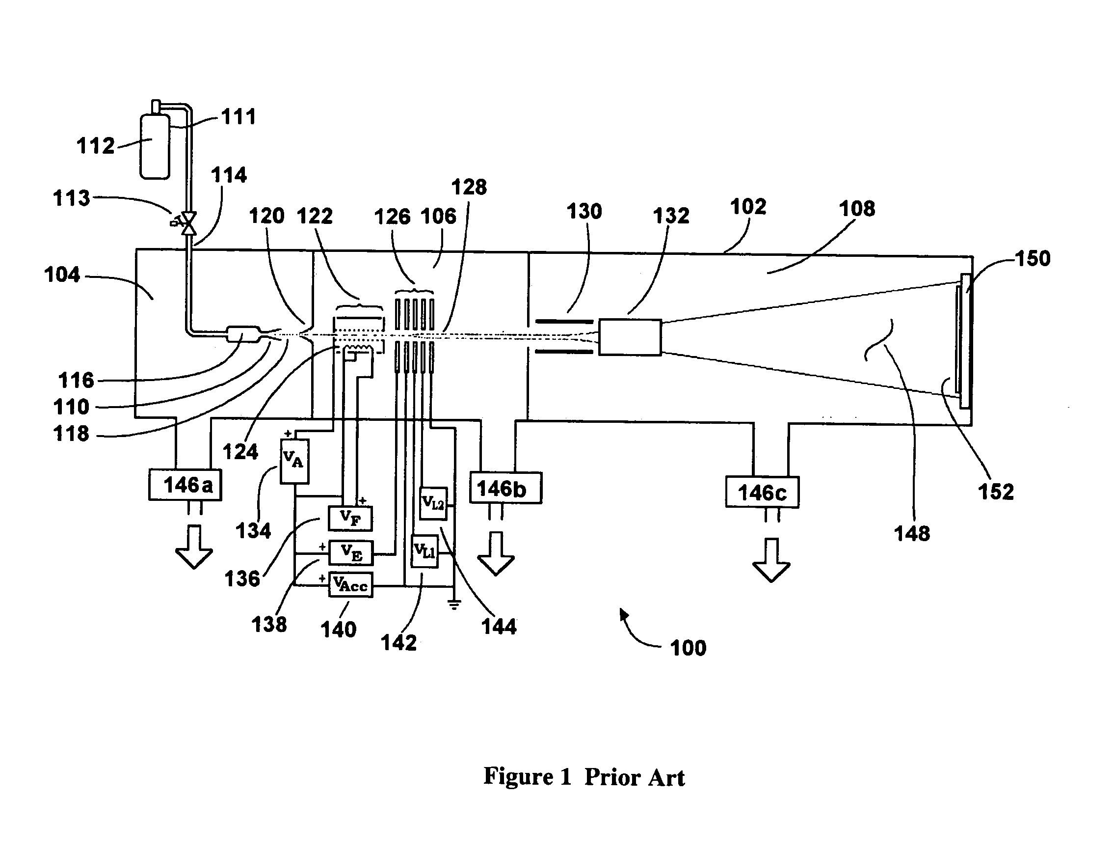
[0022]FIG. 1 shows a schematic of the basic elements of a typical configuration for a processing apparatus 100 for generating a GCIB in accordance with the present invention. Apparatus 100 may be described as follows: a vacuum vessel 102 is divided into three communicating chambers, a source chamber 104, an ionization / acceleration chamber 106, and a processing chamber 108. The three chambers are evacuated to suitable operating pressures by vacuum pumping systems 146a, 146b, and 146c, respectively. A condensable source gas 112 (for example argon or N2) stored in a gas storage cylinder 111 is admitted under pressure through gas metering valve 113 and gas feed tube 114 into stagnation chamber 116 and is ejected into the substantially lower pressure vacuum through a properly shaped nozzle 110. A supersonic gas jet 118 results. Cooling, which results from the expansion in the jet, causes a portion of the gas jet 118 to condense into clusters, each consisting of from several to several th...


PUM


Abstract

A self-aligned MISFET transistor (500H) on a silicon substrate (502), but having a graded SiGe channel or a Ge channel. The channel (526) is formed using gas-cluster ion beam (524) irradiation and provides higher channel mobility than conventional silicon channel MISFETs. A manufacturing method for such a transistor is based on a replacement gate process flow augmented with a gas-cluster ion beam processing step or steps to form the SiGe or Ge channel. The channel may also be doped by gas-cluster ion beam processing either as an auxiliary step or simultaneously with formation of the increased mobility channel.

Description

CROSS REFERENCE TO RELATED PATENT APPLICATIONS [0001] This application claims priority of U.S. Provisional Application Ser. No. 60 / 692,795 entitled “Replacement Gate Field Effect Transistor with Germanium Channel and Manufacturing Method for Same using Gas-Cluster Ion Irradiation”, filed Jun. 22, 2005, the contents of which are incorporated herein by reference.FIELD OF THE INVENTION [0002] This invention relates generally to a semiconductor field effect transistor and its manufacturing method, and more specifically, relates to a field effect transistor having a germanium channel and its manufacturing method using gas-cluster ion irradiation. BACKGROUND OF THE INVENTION [0003] The characteristics of semiconductor materials such as, silicon, germanium, silicon-germanium (SiGe), and other semiconductor materials have been exploited to form a large variety of useful devices in the fields of electronics, communications, electro-optics, and nano-technology. There has been a relentless pus...

Claims


Application Information

Patent Timeline
Patent Type & Authority Applications(United States)
IPC IPC(8): H01L21/84
CPCH01J37/3171H01L29/78684H01J2237/0812H01L21/02532H01L21/02573H01L21/02631H01L21/223H01L21/2236H01L29/1041H01L29/1054H01L29/495H01L29/51H01L29/66545H01L29/66583H01L29/6659H01L29/66651H01L29/7833H01J2237/006
Inventor BORLAND, JOHN O.SKINNER, WESLEY J.
Owner TEL EPION
Why Eureka
Try Eureka