

Semiconductor device
- Summary
- Abstract
- Description
- Claims
- Application Information
AI Technical Summary
Benefits of technology
Problems solved by technology
Method used
Image

Examples
first embodiment
Modified Example of First Embodiment
[0063] Hereinafter, explanation of a semiconductor device and its manufacture method according to a modified example of the first embodiment will be provided.
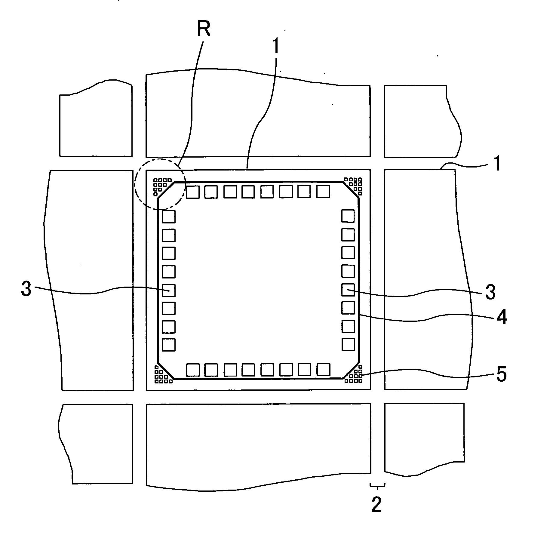
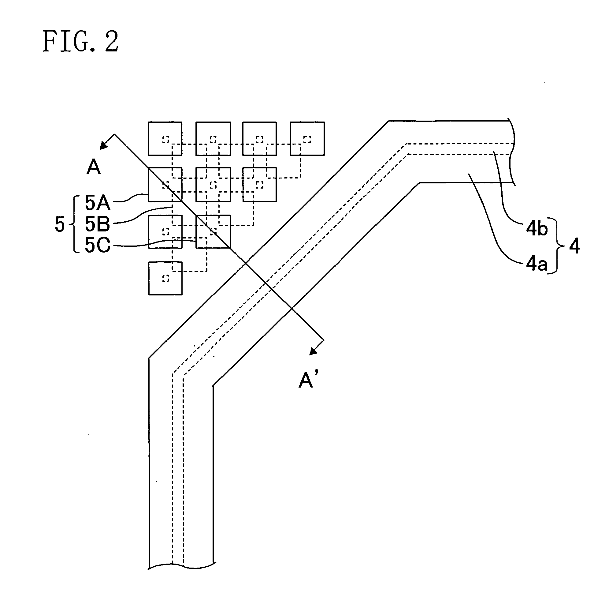
[0064] In the first embodiment described above, overlapping portions are observed between the dummy wiring structures 5A and 5B, 5C and 5B, 5B and 5D and 5B and 5E.
[0065] In the modified example, in contrast to the first embodiment, some or all of the overlapping portions of the dummy wiring structures are not provided. By so doing, the crack, peeling or the like of the interlayer insulating film derived from the mechanical or thermal stress during assembly into a package or the like is prevented with reliability while the area occupied by the dummy wiring structures is reduced.
Second Embodiment
[0066] Hereinafter, explanation of a semiconductor device and its manufacture method according to a second embodiment of the present invention will be provided with reference to the drawings.
[0067...
second embodiment
Modified Example of Second Embodiment
[0074] Hereinafter, explanation of a semiconductor device and its manufacture method according to a modified example of the second embodiment of the present invention will be provided.
[0075] In the second embodiment described above, the dummy wiring structures 51A to 51E, for example, are provided to function as the chip strength reinforcement 5.
[0076] In the modified example, however, some or all of the dummy wiring structures having portions formed in the bottommost wiring layer, e.g., the dummy wiring structures 51A to 51C, are not provided. By so doing, the crack, peeling or the like of the interlayer insulating film derived from the mechanical or thermal stress during assembly into a package or the like is prevented with reliability while the area occupied by the dummy wiring structures is reduced.
[0077] Further, in the second embodiment described above, overlapping portions are observed between the dummy wiring structures 51A and 51B, 51...
third embodiment
[0079] Hereinafter, explanation of a semiconductor device and its manufacture method according to a third embodiment will be provided with reference to the drawings.
[0080]FIG. 12 is an enlarged plan view of the upper left corner of a chip region of a semiconductor device according to the third embodiment (in particular a semiconductor chip provided with wiring structures) similar to the enlargement of the region R indicated in FIG. 1. FIG. 13 is a sectional view taken along the line B-B′ of FIG. 12 and FIG. 14 is a sectional view taken along the line C-C′ of FIG. 12. In FIGS. 12 to 14, the same components as those of the first embodiment shown in FIGS. 1 to 10 are indicated by the same reference numerals for easy explanation.
[0081] As shown in FIGS. 12 to 14, a seal ring 4 made of a first (bottommost)-layer wiring 32, second to seventh-layer wirings 40A to 40F and a cap 41 is provided at the periphery of each of the chip regions 1 in the same manner as in the first embodiment. A c...
PUM
 Abstract
Description
Claims
Application Information