

Method for producing a vertical field effect transistor
a technology of vertical field effect transistor and transistor, which is applied in the direction of transistors, semiconductor devices, electrical equipment, etc., can solve the problems of difficult production, difficult production, and difficulty in optimizing the gate structure, so as to achieve good electrical properties, simple production, and good electrical properties
- Summary
- Abstract
- Description
- Claims
- Application Information
AI Technical Summary
Benefits of technology
Problems solved by technology
Method used
Image

Examples
Embodiment Construction
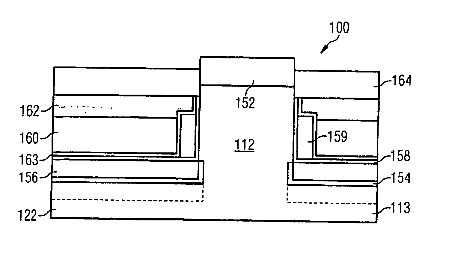
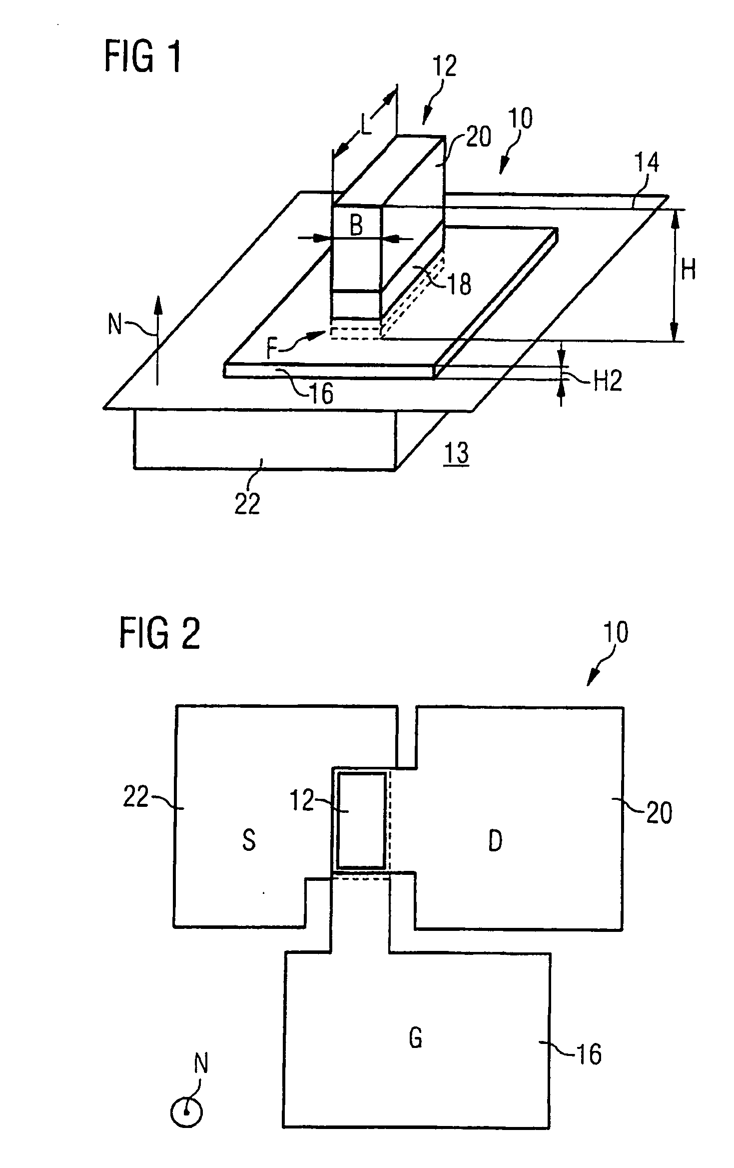
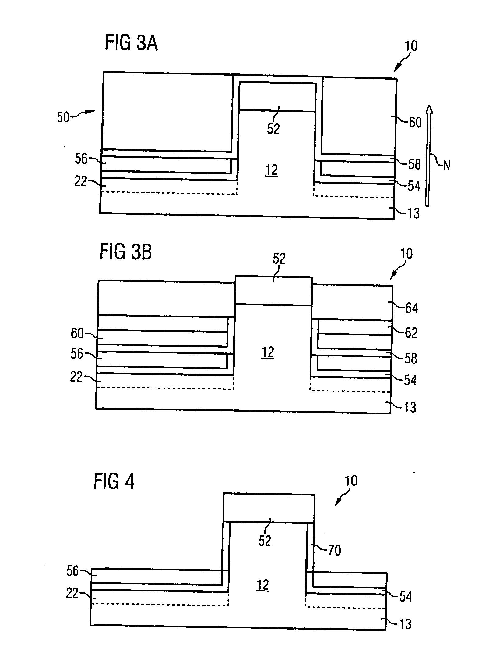
[0036]FIG. 1 shows a vertical fin field effect transistor 10 formed on a fin 12. The fin 12 has been etched from a semiconductor substrate 13, which has a planar substrate surface 14 after etching. By way of example, a silicon substrate which is initially predoped or undoped is used. The fin 12 may have a height H of 100 nanometers in the direction of the normal N to the substrate surface 14. The width B of the fin 12 is e.g. 20 nanometers. The length L of the fin 12 is e.g. 60 nanometers.
[0037] At the foot F of the fin 12 or at the base of the fin 12, a base area of the fin 12 is situated in the plane of the substrate surface 14. A gate electrode 16 encloses the fin 12 and lies parallel to and at a distance from the substrate surface 14. The distance may be 30 nanometers. The gate electrode 16 comprises doped polycrystalline silicon.
[0038] A gate dielectric 18 (not illustrated in FIG. 1) is situated between the gate electrode 16 and the fin 12. Suitable gate dielectrics are silic...
PUM
 Abstract
Description
Claims
Application Information