

Silicon dot forming method and silicon dot forming apparatus
a silicon dot and forming method technology, applied in the direction of electrolysis components, vacuum evaporation coatings, coatings, etc., can solve the problems of inability to uniformize the particle diameter and density distribution of silicon dots cannot be uniformized without difficulty, and the inability to employ low heat resistan
- Summary
- Abstract
- Description
- Claims
- Application Information
AI Technical Summary
Benefits of technology
Problems solved by technology
Method used
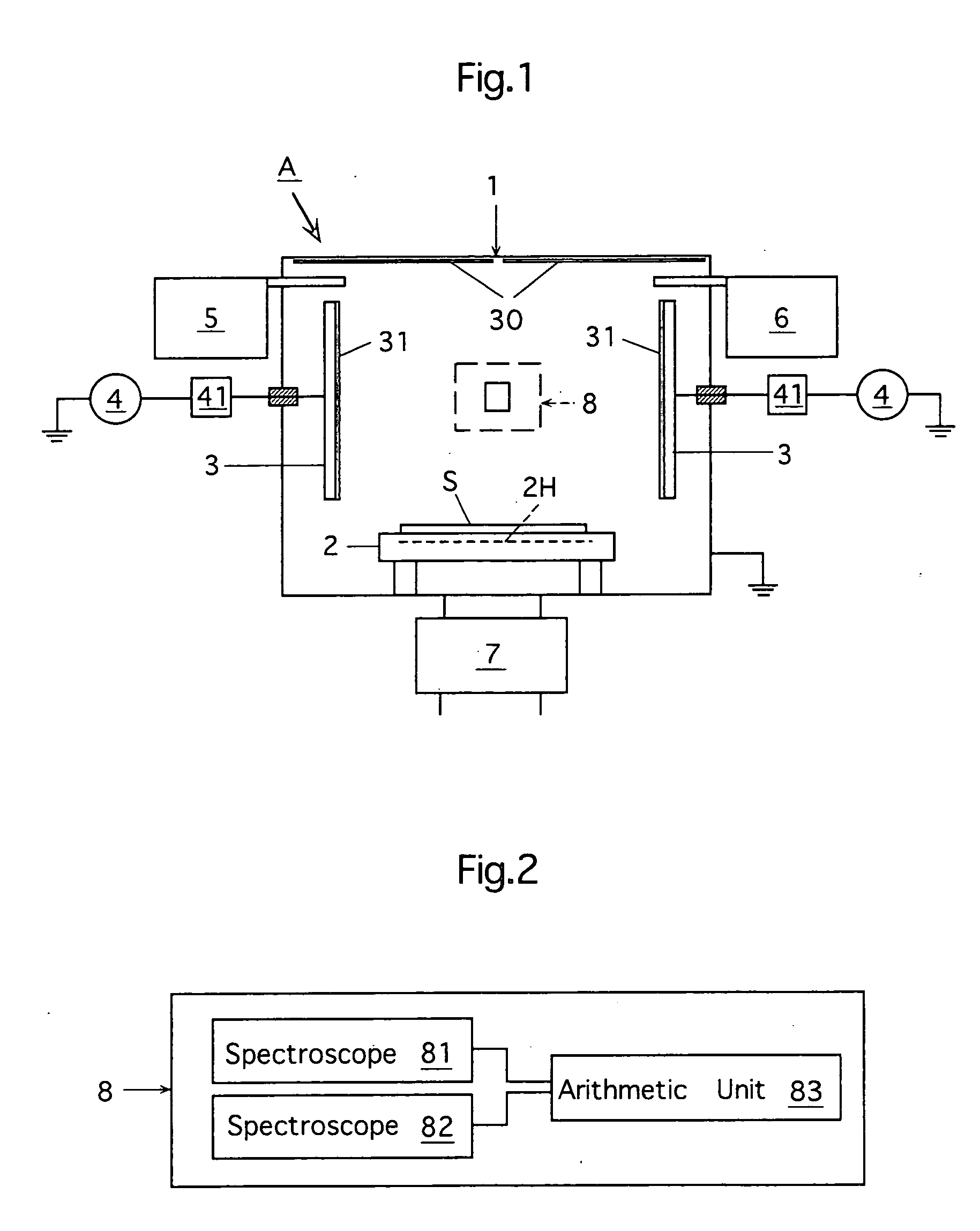
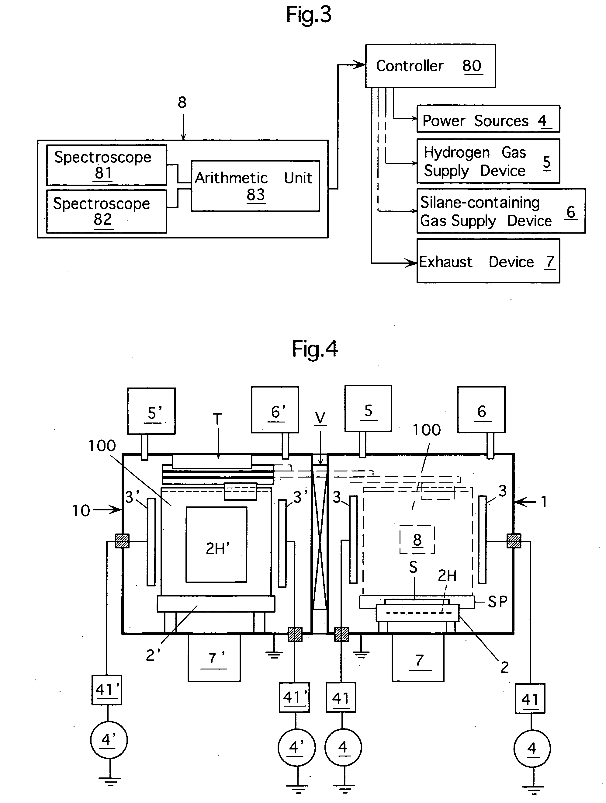
Image

Examples
experimental example
>
(1) Experimental Example 1
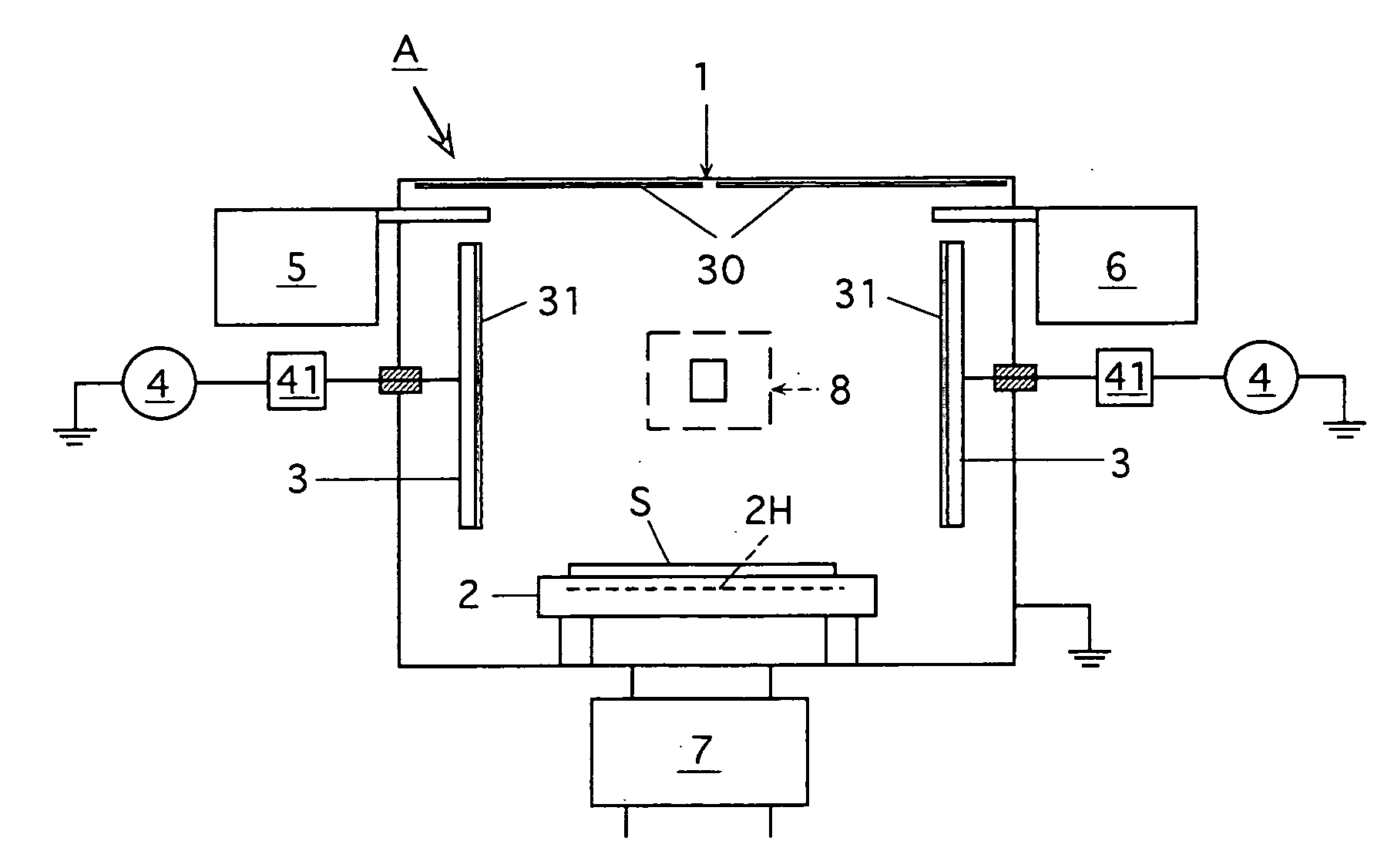
[0185] A silicon dot forming apparatus of the type shown in FIG. 1 was used. However, the silicon sputter target was not employed, and the silicon dots were directly formed on the substrate with the hydrogen gas and the monosilane gas. Dot formation conditions were as follows:
[0186] Substrate: silicon wafer coated with oxide film (SiO2)
[0187] Chamber capacity: 180 liters
[0188] High-frequency power source: 60 MHz, 6 kW
[0189] Power density: 33 W / L
[0190] Substrate temperature: 400 deg. C. (400° C.)
[0191] Inner pressure of chamber: 0.6 Pa
[0192] Hydrogen supply amount: 150 sccm
[0193] Silane supply amount: 3 sccm
[0194] Si(288 nm) / Hβ: 0.5
[0195] After forming the dots, the section of the substrate was observed with a transmission electron microscope (TEM), and it was confirmed that the silicon dots having substantially the uniform particle diameters were formed independently from each other, and these silicon dots exhibited a uniform distribution and a ...
PUM
| Property | Measurement | Unit |
|---|---|---|
| particle diameters | aaaaa | aaaaa |
| particle diameters | aaaaa | aaaaa |
| particle diameters | aaaaa | aaaaa |
Abstract
Description
Claims
Application Information