Magnetoresistive effect element and magnetic memory
a technology applied in the field of magnetic memory and effect element, can solve the problems of high power consumption, limit in allowable current density of wiring, and the inability to make the size smaller
- Summary
- Abstract
- Description
- Claims
- Application Information
AI Technical Summary
Benefits of technology
Problems solved by technology
Method used
Image

Examples
first embodiment
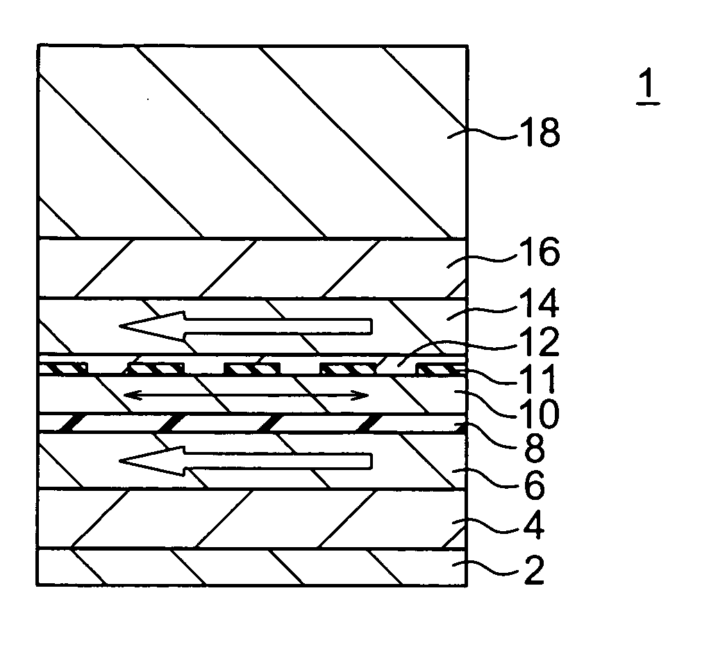
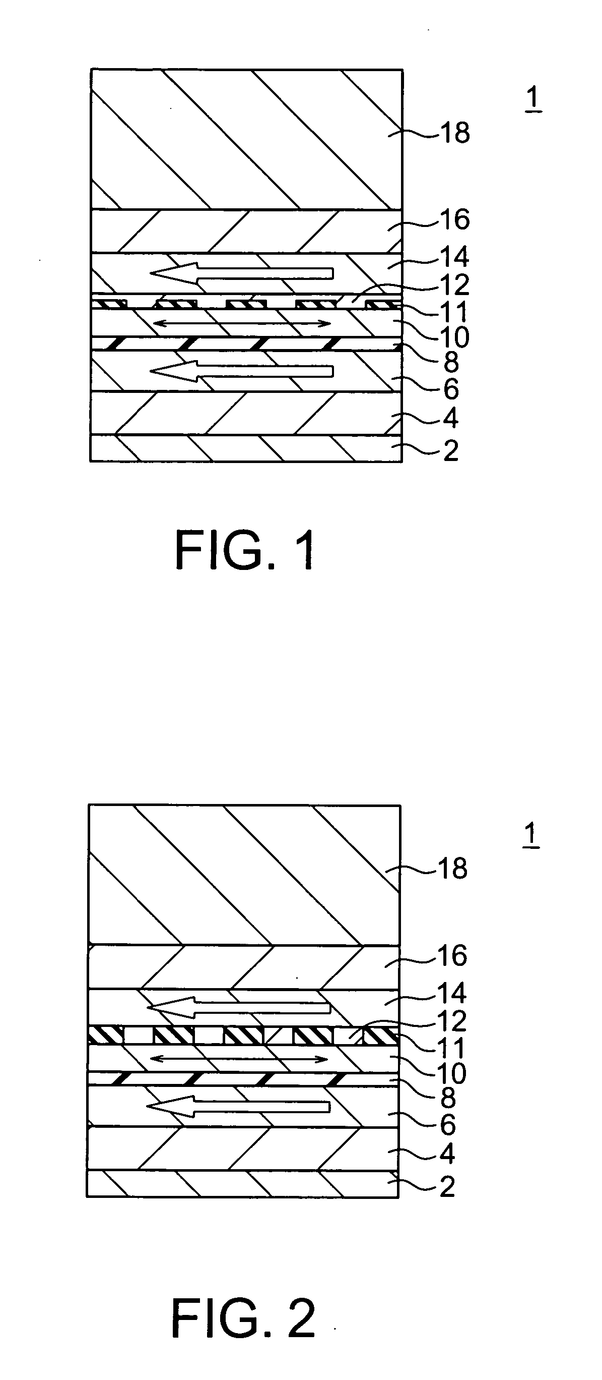
[0080] A magnetoresistive effect element according to a first embodiment of the present invention is shown in FIG. 1. The magnetoresistive effect element 1 according to this embodiment includes an antiferromagnetic layer 4 provided on an underlying layer 2, a first magnetization pinned layer 6 including a magnetic layer provided on the antiferromagnetic layer 4, in which the direction of magnetization (spin) is pinned by exchange coupling force to the antiferromagnetic layer 4, a tunnel barrier layer 8 provided on the first magnetization pinned layer 6, a magnetization free layer (magnetic recording layer) 10 having a changeable magnetization direction provided on the tunnel barrier layer 8, a second magnetization pinned layer 14 provided on the magnetic recording layer 10 so as to include a non-magnetic metal layer 12, which is divided by a dielectric 11 at least on its interface side in contact with the magnetic recording layer 10, and a magnetic layer provided on the non-magnetic...
second embodiment
[0108] A magnetoresistive effect element 1A according to a second embodiment of the present invention is shown in FIG. 9. The magnetoresistive effect element 1A according to the present embodiment has a configuration obtained by replacing the first magnetization pinned layer 6 in the magnetoresistive effect element 1 according to the first embodiment shown in FIG. 1 with a synthetic first magnetization pinned layer 6A having a three-layer structure which includes a magnetic layer 61, a non-magnetic layer 62 and a magnetic layer 63, and replacing the second magnetization pinned layer 14 with a synthetic second magnetization pinned layer 14A having a three-layer structure which includes a magnetic layer 141, a non-magnetic layer 142 and a magnetic layer 143. The magnetic layer 61 is pinned in magnetization direction by the antiferromagnetic layer 4. The magnetic layer 63 is coupled to the magnetic layer 61 antiferromagntically via the non-magnetic layer 62. The magnetic layer 143 is p...
third embodiment
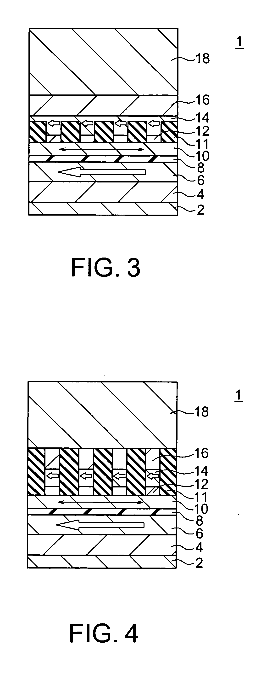
[0117] A magnetoresistive effect element according to a third embodiment of the present invention will now be described with reference to FIG. 13. The magnetoresistive effect element according to the present embodiment has a configuration in which the non-magnetic metal layer 12 is not divided by the dielectric 11 on the magnetic recording layer 10 side, but divided by the dielectric 11 on the second magnetization pinned layer 14 side in the magnetoresistive effect element according to the first embodiment shown in FIG. 1 (see FIG. 13).
[0118] In the present embodiment as well, at least a part of the non-magnetic metal layer 12 is divided by the dielectric 11 and consequently the current flowing through the non-magnetic metal layer 12 flows through a place that is not divided by the dielectric 11 in a concentrative manner in the same way as the first embodiment.
[0119] In the present embodiment as well, therefore, it becomes possible to adjust the resistance and it is possible to ob...
PUM
 Abstract
Description
Claims
Application Information
 - Generate Ideas
- Intellectual Property
- Life Sciences
- Materials
- Tech Scout
- Unparalleled Data Quality
- Higher Quality Content
- 60% Fewer Hallucinations
Browse by: Latest US Patents, China's latest patents, Technical Efficacy Thesaurus, Application Domain, Technology Topic, Popular Technical Reports.
© 2025 PatSnap. All rights reserved.Legal|Privacy policy|Modern Slavery Act Transparency Statement|Sitemap|About US| Contact US: help@patsnap.com