Group III nitride semiconductor substrate and manufacturing method thereof

a technology of nitride and semiconductor substrate, which is applied in the direction of polycrystalline material growth, crystal growth process, chemically reactive gas growth, etc., can solve the problems of insufficient stability of electric characteristic and/or optical characteristic, difficult control of resistivity, and large in-plane distribution of resistivity, etc., to achieve low dislocation density and control the effect of resistivity

Inactive Publication Date: 2007-01-18
SUMITOMO ELECTRIC IND LTD
View PDF9 Cites 46 Cited by
  • Summary
  • Abstract
  • Description
  • Claims
  • Application Information

AI Technical Summary

Benefits of technology

[0009] An object of the present invention is to provide a group III nitride semiconductor substrate having controlled resistivity and low dislocation density and a manufacturing method thereof.
[0018] As described above, according to the present invention, a group III nitride semiconductor substrate having controlled resistivity and low dislocation density and a manufacturing method thereof can be provided.

Problems solved by technology

In any of Patent Documents 2 to 4 above, however, control of the resistivity has been difficult, and in-plane distribution of the resistivity has been great.
In addition, in the group III nitride semiconductor layer or the group III nitride semiconductor layer substrate in any of Patent Documents 2 to 4 above, the dislocation density thereof cannot be as low as that of the GaN substrate obtained with the method according to Patent Document 1 above, and stability of the electric characteristic and / or optical characteristic has been insufficient.

Method used


Image

  • Group III nitride semiconductor substrate and manufacturing method thereof
  • Group III nitride semiconductor substrate and manufacturing method thereof
  • Group III nitride semiconductor substrate and manufacturing method thereof

Examples


example 1

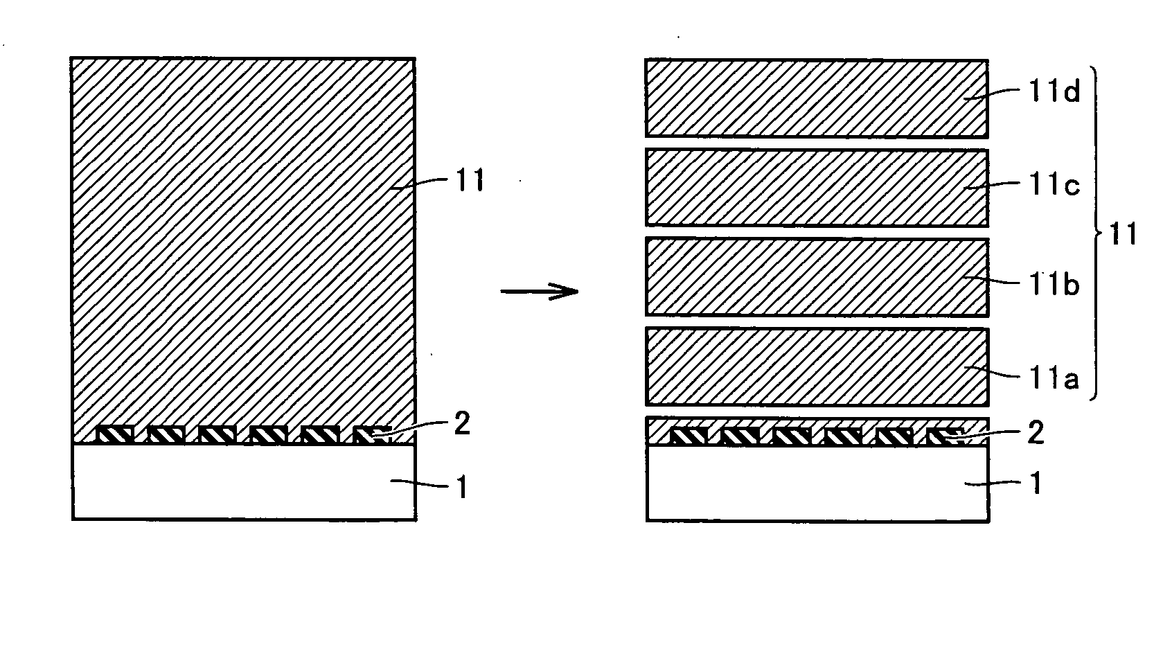
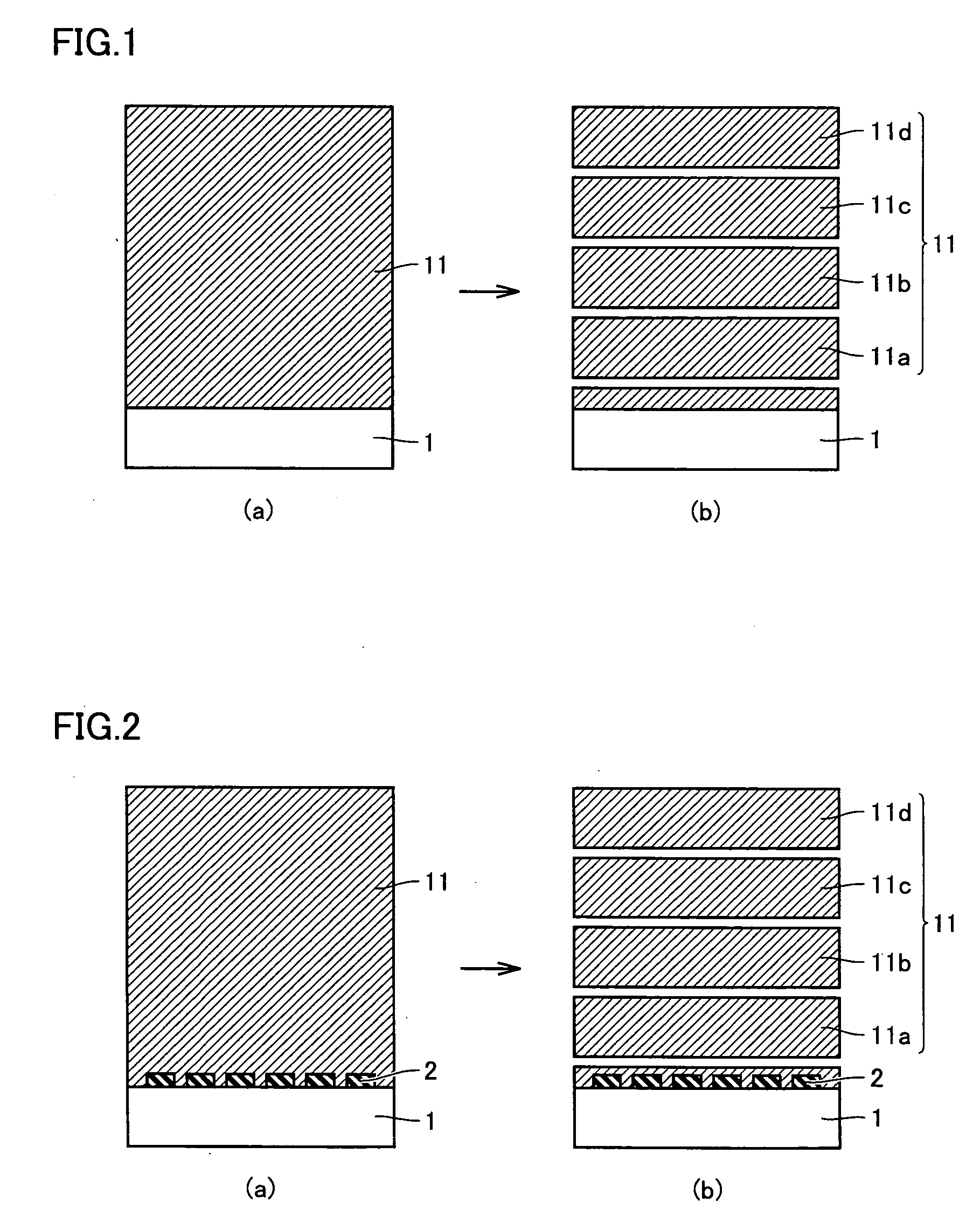
[0066] Referring to FIG. 1(a), the GaN substrate (the main surface of the substrate is at an angle of 1° in a direction of {1-100} surface with respect to (0001) surface) grown with the facet growth method (the method described in Patent Document 1) in the HVPE method was used as underlying substrate 1, and the high-resistivity GaN layer was grown as first group III nitride semiconductor layer 11 to a thickness of 2000 μm, using the HVPE method. A GaCl gas obtained by bringing an HCl gas in contact to gallium metal at 800° C. was used as the Ga source, and an NH3 gas was used as the N source. In addition, a methane gas was used as the impurity element raw material for adding C representing the impurity element. Moreover, an H2 gas was used as the carrier gas.

[0067] Here, the condition for epitaxial growth of the GaN layer using the HVPE method was set as follows: growth temperature (temperature of the underlying substrate) of 1050° C.; total pressure of 100 kPa (1.0 atmospheric pre...

example 2

[0070] The high-resistivity GaN substrate was obtained in a manner the same as in Example 1, except for using magnesium chloride (MgCl2) as the impurity element raw material. The minimum concentration of impurity element Mg in the obtained GaN substrate was 1×1018 cm−3, the in-plane distribution of the concentration of Mg 5 (maximum concentration / minimum concentration) was 2.5, the resistivity was not lower than 1×10⁵ Ω·cm, the average dislocation density was 1×106 cm−2, the surface density of the dislocation-concentrated region was not higher than 1 cm−2, the half-width of the rocking curve in X-ray diffraction was 80 arcsec, the carrier density was not higher than 1×1015 cm−3, and the absorption coefficient for light of a wavelength of 450 nm was not smaller than 50 cm−1. Table 1 summarizes the result.

example 3

[0071] The high-resistivity GaN substrate was obtained in a manner the same as in Example 1, except for using an iron chloride (FeCl2) gas generated as a result-of reaction of iron and hydrochloric gas as the impurity element raw material. The 15 minimum concentration of impurity element Fe in the obtained GaN substrate was 1×1018 cm−3, the in-plane distribution of the concentration of Fe (maximum concentration / minimum concentration) was 2.0, the resistivity was not lower than 1×10⁷ Ω·cm, the average dislocation density was 1×106 cm−2, the surface density of the dislocation-concentrated region was not higher than 1 cm−2, the half-width of the rocking curve in X-ray diffraction was 80 arcsec, the carrier density was not higher than b 1×1015 cm−3, and the absorption coefficient for light of a wavelength of 450 nm was not smaller than 50 cm−3. Table 1 summarizes the result.


PUM

PropertyMeasurementUnit
thicknessaaaaaaaaaa
resistivityaaaaaaaaaa
angleaaaaaaaaaa

Abstract

A method of manufacturing a group III nitride semiconductor substrate includes the growth step of epitaxially growing a first group III nitride semiconductor layer on an underlying substrate, and the process step of forming a first group III nitride semiconductor substrate by cutting and / or surface-polishing the first group III nitride semiconductor layer. In the growth step, at least one element selected from the group consisting of C, Mg, Fe, Be, Zn, V, and Sb is added as an impurity element by at least 1×1017 cm−3 to the first group III nitride semiconductor layer. A group III nitride semiconductor substrate having controlled resistivity and low dislocation density and a manufacturing method thereof can thus be provided.

Description

BACKGROUND OF THE INVENTION [0001] 1. Field of the Invention [0002] The present invention relates to a group III nitride semiconductor substrate having controlled resistivity and low dislocation density and a manufacturing method thereof. [0003] 2. Description of the Background Art [0004] In recent years, development of a group III nitride semiconductor substrate suitable as a substrate of various semiconductor devices such as an optical device and an electronic device, that has controlled resistivity, low dislocation density, and stable electric characteristic and / or optical characteristic, has been demanded. [0005] As a method of significantly lowering dislocation density of a group III nitride semiconductor substrate, for example, Japanese Patent Laying-Open No. 2001-102307 (hereinafter, referred to as Patent Document 1) proposes a method of lowering dislocation density in a region other than a dislocation-concentrated region (referred to as low dislocation region here and herein...

Claims


Application Information

Patent Timeline
Patent Type & Authority Applications(United States)
IPC IPC(8): H01L33/00H01L21/00C30B29/38H01L21/205
CPCC30B25/02C30B29/406H01L21/0237H01L21/02433H01L21/02647H01L21/02573H01L21/02581H01L21/0262H01L21/0254
Inventor OKAHISA, TAKUJINAKAHATA, HIDEAKINAKAHATA, SEIJI
Owner SUMITOMO ELECTRIC IND LTD
Why Eureka
Try Eureka