Self-luminous flat-panel display

Inactive Publication Date: 2007-01-25
HITACHI DISPLAYS
View PDF2 Cites 6 Cited by
  • Summary
  • Abstract
  • Description
  • Claims
  • Application Information

AI Technical Summary

Benefits of technology

[0013] The present invention has been therefore made for solving the foregoing problems associated with the conventional techniques, and an object of the invention is to provide a self-luminous flat-panel display apparatus using an electron source formed of: a carbon nanotube or any other appropriate nanomaterial that reduces wiring resistance, even in large display apparatuses with screen sizes of about 40 inches or more, is sufficiently high in electrical response characteristics, and can generate uniform light-emission patterns.
[0014] In order to attain the above object, a self-luminous flat-panel display apparatus according to the present invention suppresses any vertical dimensional differences between surface depressions and projections of a cathode in pixels formed in central and peripheral sections of a display region, to 1 μm or less. Also, an electron source layer-made of a nanomaterial is formed on the surface of the cathode, and the cathode itself is fabricated using a printing method. Thus, it becomes possible to realize a film thickness of several micrometers, reduce wiring resistance, and ensure high-speed response characteristics, and hence to solve the problems described in “BACKGROUND OF THE INVENTION.”
[0015] In another self-luminous flat-panel display apparatus according to the present invention can, preferably under such a configuration as described above, not only a shape and average particle size of the metallic particles contained in the printing paste used to form a cathode, but also a composition of the printing paste are optimized to suppress any vertical dimensional differences between surface depressions and projections of the cathode to 0.5 μm or less and realize uniform emission of light. The problems described in “BACKGROUND OF THE INVENTION” can thus be solved.
[0016] Accordingly, a self-luminous flat-panel display apparatus can be easily manufactured using a coating process, such as a screen-printing process, that is expected to achieve cost reduction.

Problems solved by technology

With sputtering, however, it is impossible to form a film thickness of several micrometers (μm).
Sputtering, therefore, has had a problem in that since line resistance increases, large display apparatuses cannot transmit high-speed electrical signals.
These printing methods, however, have had problems in that vertical dimensional differences between the depressions and projections on the film surface are augmented to range from 3 μm to 5 μm, and hence that the height of the carbon nanotube formed as an electron source on the surface of the cathode becomes nonuniform and the density of an emission point decreases.

Method used


Image

  • Self-luminous flat-panel display
  • Self-luminous flat-panel display
  • Self-luminous flat-panel display

Examples


first preferred embodiment

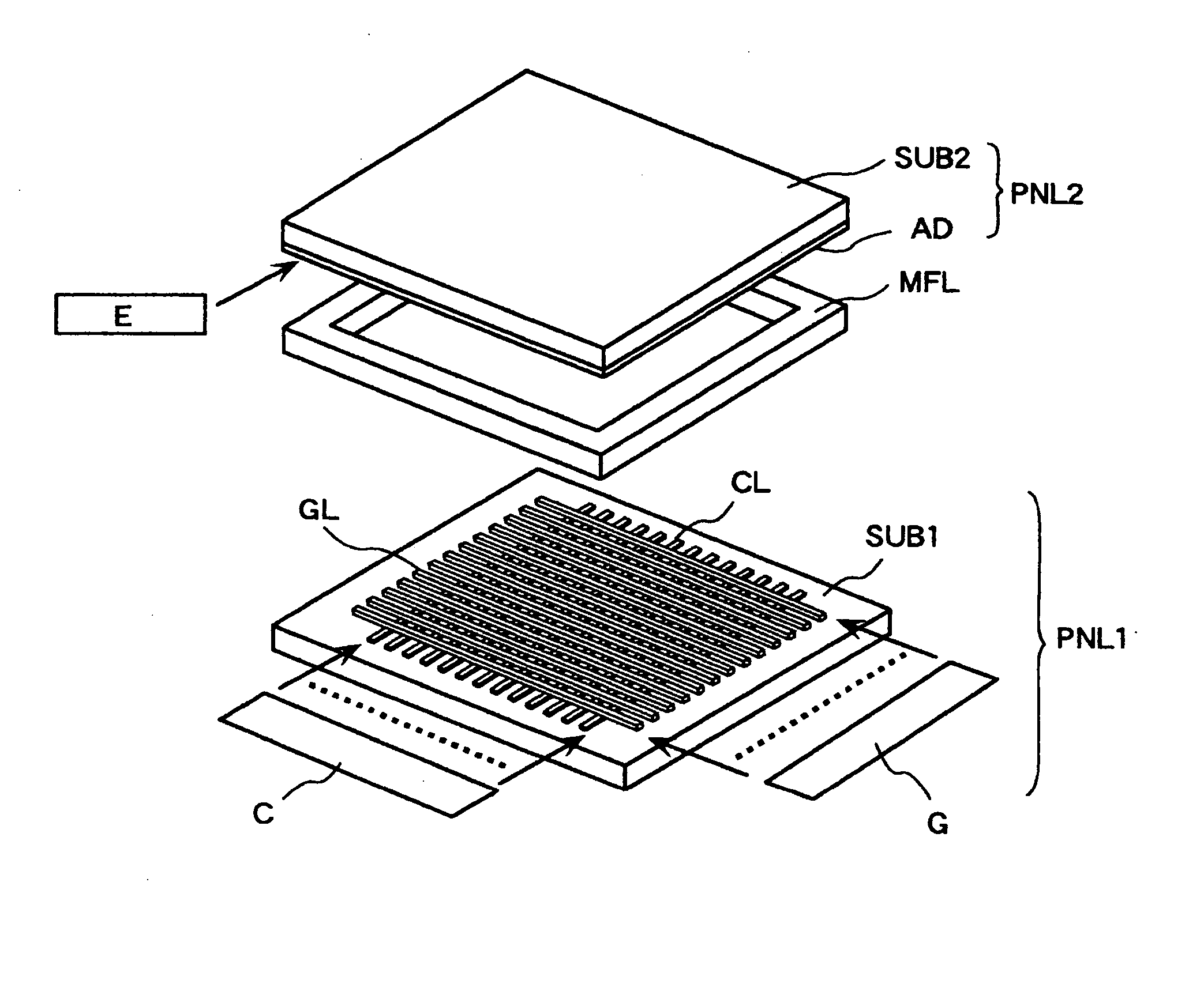
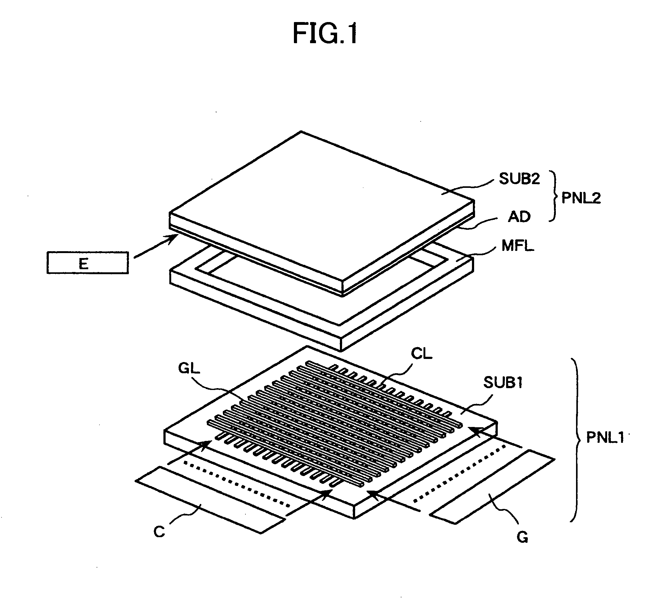
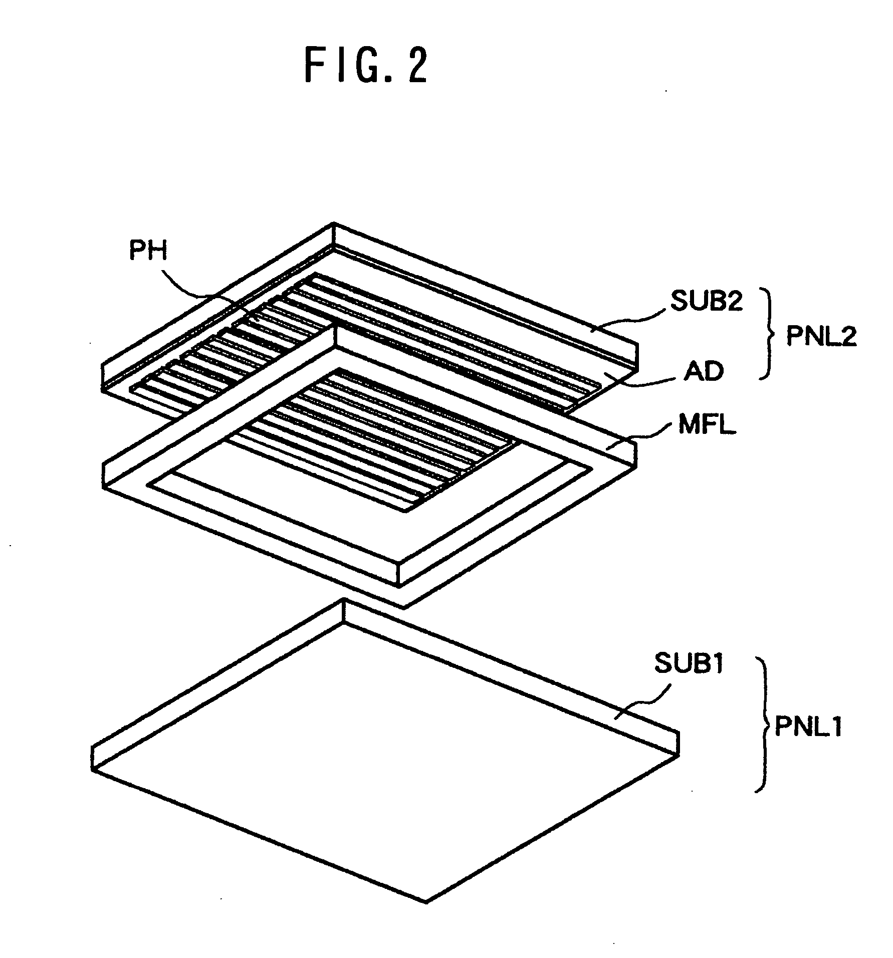
[0049]FIGS. 1 and 2 are schematic views illustrating structurally a first embodiment of a self-luminous flat-panel panel display apparatus according to the present invention, FIG. 1 being an essential section development perspective view of the self-luminous flat-panel display apparatus as viewed from an oblique upward direction, and FIG. 2 being an essential section development perspective view of the self-luminous flat-panel display apparatus as viewed from an oblique downward direction. A rear substrate SUB 1 that forms a rear panel PNL 1, and a front substrate SUB 2 that forms a front panel PNL 2 are adhesively attached to each other via a sealing frame MFL, thereby to constitute the self-luminous flat-panel display apparatus.

[0050]FIG. 3 is an essential section plan view looking at an inner surface of the rear substrate SUB 1 of the self-luminous flat-panel display apparatus from an upward direction. In FIG. 3, a large number of cathodes CL extending in one (first) direction a...

second preferred embodiment

[0070] FIGS. 11 to 14 show another structural example of a rear panel in a self-luminous flat-panel display apparatus according to the present invention, and fabrication process steps for implementing this structural example. Subpixels of an electron source array are described in detail in accordance with the figures.

[0071] First, as shown in FIG. 11, the surface of a rear substrate SUB 1 using a glass sheet as its preferred material is coated with an electrode-forming silver paste created from an organic solvent which contains silver fine particles and lead glass particles. This coating process is performed in stripe form by means of screen-printing, and after the coating process, the surface is baked to form a cathode CL and gate electrodes GL at the same time. The cathode CL and the gate electrodes GL are formed on essentially the same plane of the rear substrate SUB 1. The electrode-forming silver paste consists of silver fine particles with an average particle size of about 0....


PUM


Abstract

This invention relates to a field-emission-type flat-panel display apparatus that obtains an image by causing the electrons emitted from each of electron sources arranged in matrix form to impinge upon the phosphors formed on a phosphor screen. A carbon nanotube is used as an electron source material in this flat-panel display apparatus, and the electron sources are formed by printing. The vertical sizes of the depressions and projections on the surface of each electron source which has been formed by printing are suppressed to a value equal to or less than 1 μm, preferably, equal to or less than 0.5 μm. This makes it possible to obtain a flat-panel display apparatus of stable emission characteristics.

Description

CLAIM OF PRIORITY [0001] The present application claims priority from Japanese Application JP2005-155031 filed on May 27, 2005, the content of which is hereby incorporated by reference into this application. FIELD OF THE INVENTION [0002] The present invention relates generally to display apparatuses that use electron emission into a vacuum. More particularly, the invention relates to a self-luminous flat-panel display apparatus that includes: a rear panel equipped with cathodes each having an electron source constructed of a nanomaterial, and with gate electrodes each controlling the quantity of electron emission from the electron source; and a front panel equipped with multicolored phosphor layers each emitting light by means of excitation of the electrons acquired from the rear panel, and with anodes. BACKGROUND OF THE INVENTION [0003] Color cathode-ray tubes have long been commonly used in display apparatuses excellent in both brightness and resolution. However, the tendency towa...

Claims


Application Information

Patent Timeline
IPC IPC(8): H01J63/04H01J1/62
CPCH01J31/127H01J1/68
Inventor OKAI, MAKOTOYAMAZAKI, TETSUYASASAKI, SUSUMUMUNEYOSHI, TAKAHIKOYAGUCHI, TOMIOISHIKAWA, JUNHAYASHI, NOBUAKI
Owner HITACHI DISPLAYS
Why Eureka
Try Eureka