Optical device, optical device apparatus, camera module, and optical device manufacturing method

a manufacturing method and optical device technology, applied in the field of optical devices, can solve the problems of imposing a severe limitation on the number of electrode terminals that can be formed, cannot prevent phenomena, and cannot prevent phenomena, etc., to achieve excellent optical characteristics, simple manufacturing method, and reduce thickness and size

Active Publication Date: 2007-01-25
PANNOVA SEMIC
View PDF10 Cites 46 Cited by
  • Summary
  • Abstract
  • Description
  • Claims
  • Application Information

AI Technical Summary

Benefits of technology

[0020] As described above, in the optical device of the present invention, the transparent member is directly mounted on the principal face of the optical element, achieving reduction in thickness and size. Reflected light from an electrode terminal provided in the outer peripheral part of the region for light detection or emission or a wire lead thereof enters to the region for light detection or emission to serve as stray light. In the optical device of the present invention, however, this phenomenon can be suppressed. As a result, an optical device inviting neither a smear nor a flare and excellent in optical characteristic can be realized by the simple manufacturing method.

Problems solved by technology

Though the cap glasses can be manufactured easily, such a phenomenon cannot be prevented in the first conventional example.
This imposes a severe limitation on the number of the electrode terminals that can be formed.
Also, in this example, the phenomenon cannot be prevented in which reflected light from an electrode terminal provided in the peripheral part, a wire lead connected thereto, or the like enters into the imaging region to cause a smear or a flare.

Method used


Image

  • Optical device, optical device apparatus, camera module, and optical device manufacturing method
  • Optical device, optical device apparatus, camera module, and optical device manufacturing method
  • Optical device, optical device apparatus, camera module, and optical device manufacturing method

Examples


embodiment 1

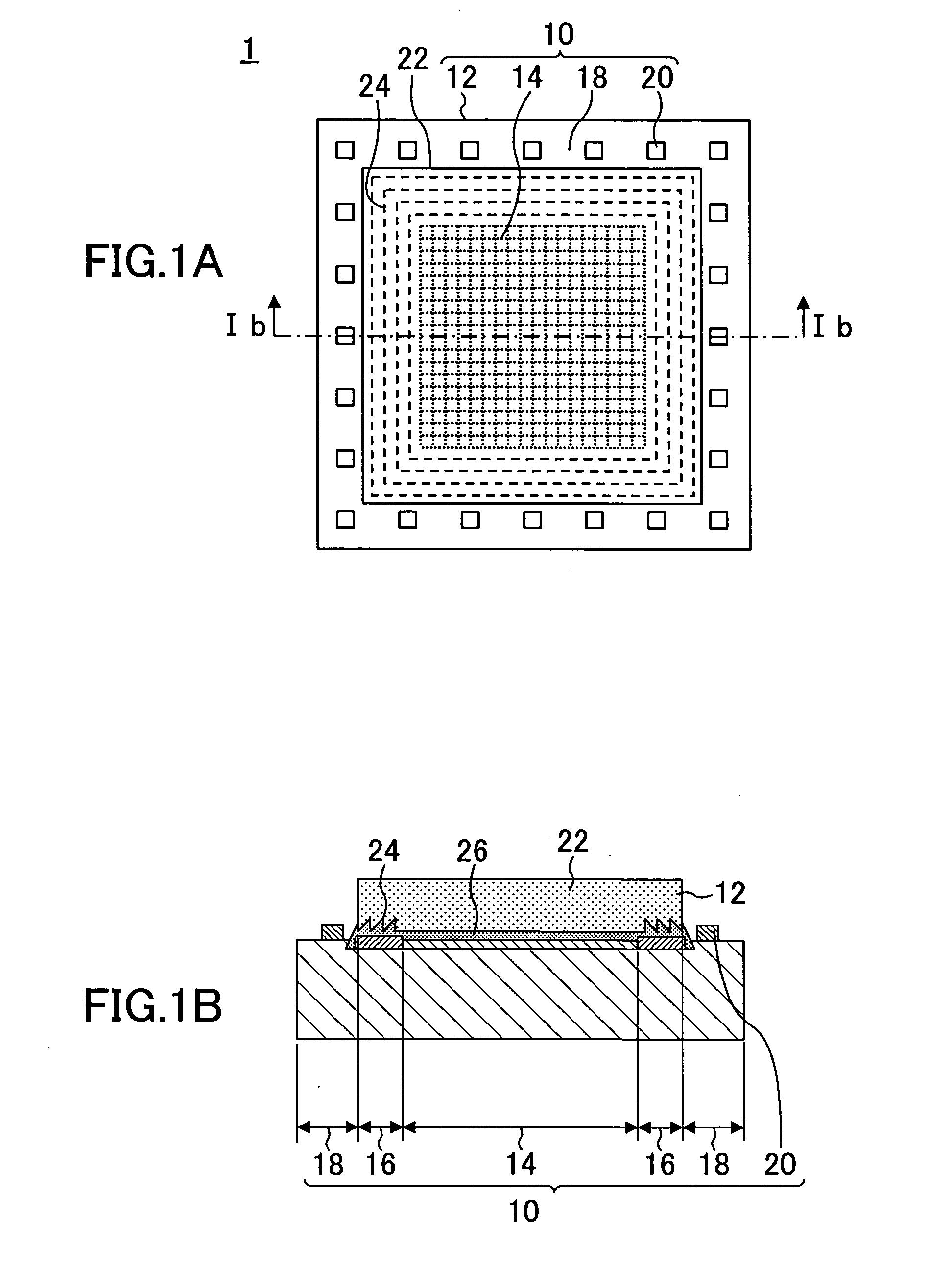
[0035]FIG. 1A is a plan view showing an optical device 1 according to Embodiment 1 of the present invention, and FIG. 1B is a section taking along the line Ib-Ib in FIG. 1A.

[0036] As shown in FIG. 1A and FIG. 1B, the optical device 1 of the present embodiment includes an optical element 10 including, in a semiconductor substrate 12, a light detecting region 14, a peripheral circuit region 16, and electrode region 18 including a plurality of electrode terminals 20, a transparent member 22, and a transparent resin adhesive 26 for making the transparent member 22 to adhere and be fixed to the optical element 10. At least one of a light receiving element and a light emitting element is provided as the optical element 10 in the optical device 1. The light receiving element is an image sensor such as a CMOS sensor, a CCD sensor, or the like while the light emitting element is, for example, a laser, a light emitting diode, or the like. In the case where the optical element 10 serves as th...

first modified example

[0065]FIG. 6A is a plan view showing an optical device according to First Modified Example of the present embodiment, and FIG. 6B is a section taking along the line VIb-VIb in FIG. 6A.

[0066] As shown in FIG. 6A and FIG. 6B, an optical device 2 of First Modified Example is the same as the optical device 1 of Embodiment 1 except the point that a transparent member 60 different in shape from that in Embodiment 1 is formed on the optical element 10 used in Embodiment 1.

[0067] In the optical device 2 of the present modified example, the transparent member 60 is fixed on the optical element 10 by means of the transparent resin adhesive 26 so as to cover the entirety of the circuit formation face of the optical element 10. Wherein, opening parts 64 having a dimension in plan larger than the electrode terminals 20 of the optical element 10 are formed at parts overlapped with the electrode terminals 20. Accordingly, the dimension in plan of the transparent member 60 is the same as the dime...

second modified example

[0072]FIG. 7A is a plan view showing an optical device 3 according to Second Modified Example of the present embodiment, and FIG. 7B is a section taking along the line VIIb-VIIb in FIG. 7A.

[0073] The optical device 3 of the present modified example is an optical device 2 of First Modified Example of which part is further modified. In the optical device 2 of First Modified Example, the opening parts 64 of the transparent member 60 are slightly larger than the electrode terminals 20 of the optical element 10. In contrast, in the optical device 3 of Second Modified Example, as shown in FIG. 7A and FIG. B, opening parts 71 form squared C-shapes in plan by cutting parts including regions of the transparent member 70 which are overlapped with the electrode terminals 20. Accordingly, the outer shape of the transparent member 70 is a rectangle in plan with indentations. The elements other than the transparent member 70 and the manufacturing method thereof are the same as those of the optic...


PUM


Abstract

An optical device includes an optical element, a transparent member arranged on the optical element, and a transparent resin adhesive for causing the transparent member to adhere and be fixed onto a circuit formation face of the optical element. The optical device includes a light detecting region having a plurality of micro lenses, a peripheral circuit region formed in the outer peripheral part of the light detecting region, and an electrode region formed at the outer peripheral part of the peripheral circuit region. A roughed region in a saw-toothed shape in section is formed in part of a face of the transparent member which adheres to the optical element, the part being overlapped with the outer peripheral part of the light detecting region as viewed in plan.

Description

BACKGROUND OF THE INVENTION [0001] 1. Field of the Invention [0002] The present invention relates to an optical device and a method for manufacturing it. [0003] 2. Prior Art [0004] In association with recent progress of miniaturization, thinning, lighting, and multi-functionalization of electronic appliances, the mainstream of semiconductor device implementation technology has been being transferred from conventional package type implementation to flip chip implementation which is implementation in a unit of a bear chip or a CSP to a circuit board or the like. Such implementation is under examination in semiconductor imaging devices. [0005] For example, the following technique was proposed as a structure and a manufacturing method thereof for attaining a lightweight semiconductor imaging device at low cost. [0006] First, a cap glass is attached to a substrate so as to cover an imaging element section of each chip in the form of a wafer. Wherein, an attached part of the cap glass is ...

Claims


Application Information

Patent Timeline
Patent Type & Authority Applications(United States)
IPC IPC(8): G02B13/16H01L27/14H04N5/335H04N5/357
CPCG02B3/0006G02B3/0056H01L27/14618H01L27/14687H01L27/14632H01L27/14685H01L27/14625H01L2224/32225H01L2224/48091H01L2224/48227H01L2224/73265H01L2224/45144H01L2924/00014H01L2924/00
Inventor MINAMIO, MASANORIHARADA, YUTAKAFUKUDA, TOSHIYUKI
Owner PANNOVA SEMIC
Why Eureka
Try Eureka