Materials and methods for creating imaging layers

Active Publication Date: 2007-01-25
WISCONSIN ALUMNI RES FOUND
View PDF5 Cites 72 Cited by
  • Summary
  • Abstract
  • Description
  • Claims
  • Application Information

AI Technical Summary

Benefits of technology

[0005] The present invention provides patterned features of dimensions of less than 50 nm on a substrate. According to various embodiments, the features may be “Manhattan” style structures, have high aspect ratios, and/or have atomically smooth surfaces. The patterned features are made from polymer brushes grafted to a substrate. In some embodiments, the dimensions of the features may be determined by adjusting the grafting density and

Problems solved by technology

As feature dimensions shrink to below 50 nm, however, the use of CARs poses significant new challenges with respect to prob

Method used


Image

  • Materials and methods for creating imaging layers
  • Materials and methods for creating imaging layers
  • Materials and methods for creating imaging layers

Examples


Example

Example 1

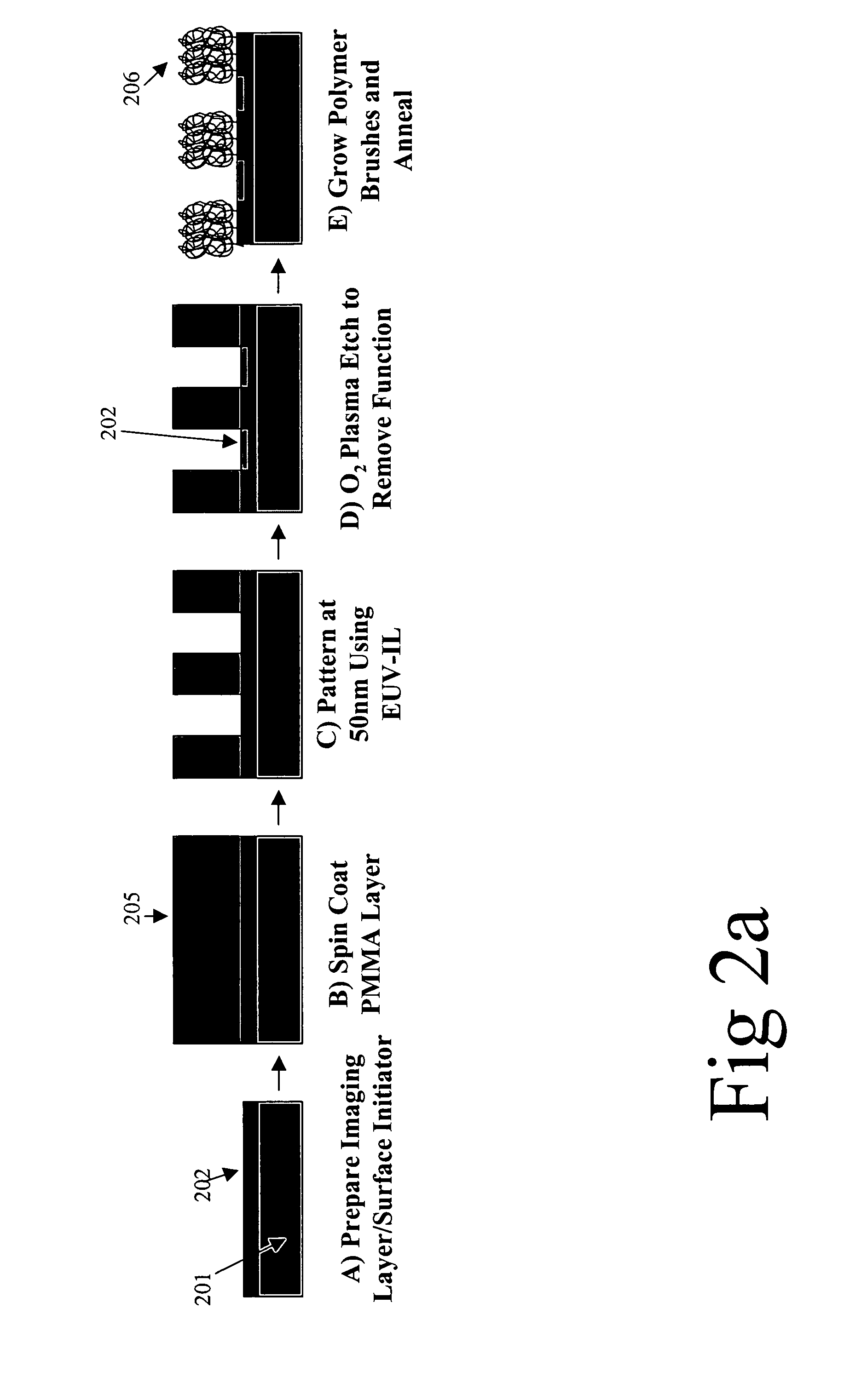
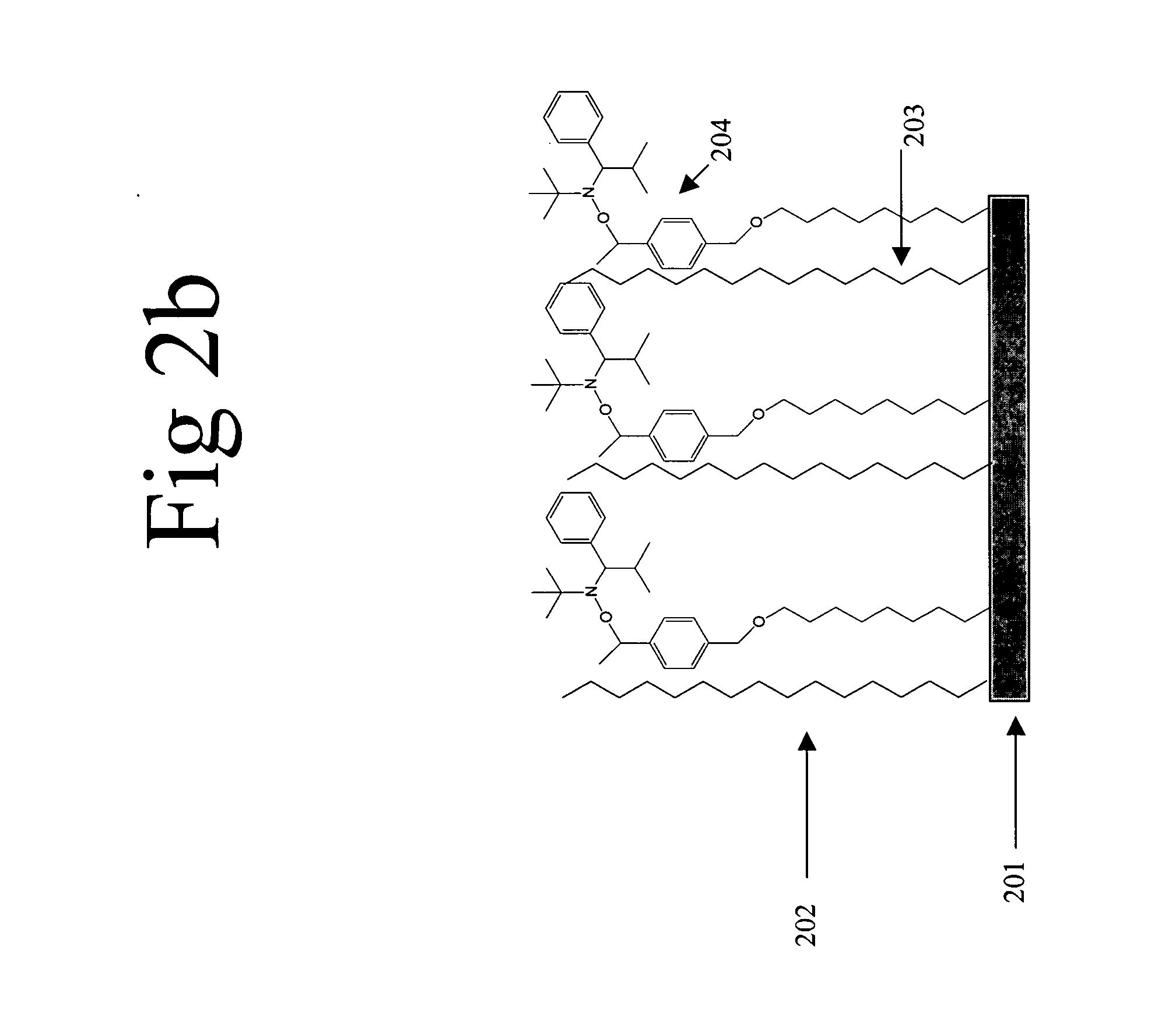
[0056] Substrates with an imaging layer with initiator sites of grafting density G of 0.7 chains / nm2 were prepared as discussed above with respect to FIG. 2. A PMMA photoresist layer was spun on the imaging layer and patterned using EUV-IL. The resulting pattern on each substrate was a 1:150 nm linear pattern (i.e. 50 nm lines, spaced 50 nm apart). Polystyrene patterned brushes were then grown on the substrates. The reaction was stopped at the desired molecular weight and the samples were placed in a Soxhlet extractor and exposed to a toluene solvent for 48 hours. The samples were then removed from the solvent and dried.

[0057] Patterned brushes of various molecular weights were grown and observed. Molecular weight was increased until feature collapse was observed. Feature collapse is the point at which discrete features are no longer observed. FIGS. 9a-c show SEM images of the patterned brushes with various molecular weights. The average molecular weight of the patterned ...

Example

Example 2

[0058] Substrates with a 50 m 1:1 linear pattern and a grafting density of 0.25 chains / nm2 were prepared as in Example 1. FIGS. 10a-c show SEM images of the patterned brushes with various molecular weights.

[0059] The average molecular weight of the patterned brushes in FIG. 10a is 17,230 g / mol with PDI equal to 1.25. Feature height is 8 nm. The patterned features are well ordered with few defects. As with the 0.7 chaims / nm2 in Example 1, increasing M results in taller features and more defects. FIG. 10b shows a patterned brush with brushes of 30,290 g / mol and a PDI of 1.40. Height is 13 nm. The patterned features in FIG. 10b have more defects than those in FIG. 10a. The patterned brushes in FIG. 10c have a molecular weight of 37,810 g / mol, a PDI of 1.4 and a height of 16 nm. Defects are observed throughout the pattern. Feature collapse occurred at an M of 44,000 g / mol and a feature height of about 20 nm.

[0060] The results shown in Examples 1 and 2 demonstrate that lower ...

Example

Example 3

[0062] Substrates with a 25 nm 1:1 linear pattern and a grafting density of 0.30 chains / nm2 were prepared as described in Example 1. FIGS. 11a and 11b show SEM images of the patterned brushes with various molecular weights. The brushes in FIG. 11b have a M of 17,380 g / mol, a PDI of 1.34 and a height of 10 n-m. Large areas of defects are observed. FIG. 11b shows patterned brushes with M of 24,840, a PDI of 1.33 and a height of 12 nm. As with the pattern shown in FIG. 11a, large areas of defects are observed. Feature collapse occurred at an M of 30,250 g / mol and a height of about 14 nm. Defects due to chains bridging the gaps occurred at all molecular weights. This is due to the fact that gaps of the patterns are 25 nm. Increasing the gap width (i.e. changing the pitch) for a feature size of 25 nm would result in fewer defects.


PUM

PropertyMeasurementUnit
Sizeaaaaaaaaaa
Sizeaaaaaaaaaa
Widthaaaaaaaaaa

Abstract

The present invention provides patterned features of dimensions of less than 50 nm on a substrate. According to various embodiments, the features may be “Manhattan” style structures, have high aspect ratios, and/or have atomically smooth surfaces. The patterned features are made from polymer brushes grafted to a substrate. In some embodiments, the dimensions of the features may be determined by adjusting the grafting density and/or the molecular weight of the brushes. Once the brushes are patterned, the features can be shaped and reshaped with thermal or solvent treatments to achieve the desired profiles. The chemical nature of the polymer brush is thus independent of the patterning process, which allows for optimization of the polymer brush used for specific applications. Applications include masks for pattern transfer techniques such as reactive ion etching.

Description

CROSS-REFERENCE TO RELATED APPLICATION [0001] This application claims priority under 35 USC § 119(e) from U.S. Provisional Application No. 60 / 664,797, filed Mar. 23, 2005, hereby incorporated by reference in its entirety and for all purposes.FIELD OF THE INVENTION [0002] The present invention relates to nanoscale patterning. More specifically, the present invention relates to creating nanoscale patterned features using polymer brushes. BACKGROUND OF THE INVENTION [0003] Production of faster and more powerful integrated circuits in the microelectronics industry requires that the dimensions of devices patterned using advanced lithography continue to decrease. Current high-resolution lithographic processes are based on chemically amplified resists (CARs) and are routinely used to pattern features with dimensions less than 100 nm. As feature dimensions shrink to below 50 nm, however, the use of CARs poses significant new challenges with respect to problems such as line edge roughness, c...

Claims


Application Information

Patent Timeline
IPC IPC(8): C12M3/00G01N33/549H01L21/00
CPCB82Y10/00B82Y30/00C08J7/12C08J7/16G03F1/003H01L21/3086G03F7/165H01L21/0271H01L21/3081H01L21/3083G03F1/68B81C1/00404B82B3/0014
Inventor NEALEY, PAUL F.JAIN, TUSHAR S.EDWARDS, ERIK W.DE PABLO, JUAN J.
Owner WISCONSIN ALUMNI RES FOUND
Why Eureka
Try Eureka