Flip chip interface including a mixed array of heat bumps and signal bumps

a chip interface and signal bump technology, applied in the field of electrical connectors and heat connectors, can solve the problems of many packages not supporting speeds greater than 200 mpbs, affecting the cooling performance of chips, and affecting the performance of chips, so as to achieve the effect of increasing the density of cooling the chip

Inactive Publication Date: 2007-02-01
SALMON TECH
View PDF99 Cites 31 Cited by
  • Summary
  • Abstract
  • Description
  • Claims
  • Application Information

AI Technical Summary

Benefits of technology

[0006] A flip chip interface is described for attaching a chip to a substrate. Each flip chip connector has a pillar in well (PIW) construction. The pillars are formed at input / output (I / O) pads of the chip. A matching well is provided in the substrate for each pillar on the chip. The wells are filled with conductive material that may be a dry powder during testing and rework, converting to melted solder in a finished module. A mixed array of PIW connectors is provided at the chip-to-substrate interface. The mixed array includes signal pillars carrying signals or power, and heat pillars at increased density for cooling the chip. Three levels of cooling are provided, ranging from 9W / cm2 using signal pillars, to 160 W / cm2 using heat pillars, to over 1000W / cm2 using copper slugs on the back side of the chip for hot spots.

Problems solved by technology

The slow rate of development of integration methods compared with silicon fabrication has resulted in an integration gap; this gap has dimensions of cost, performance, cooling, and scalability.
Digital IC chips can now operate at signaling rates of 10 Gbps while many packages do not support speeds greater than around 200 Mpbs.
Cooling has become critical.
Modern servers typically have bulky finned aluminum heat sinks surrounding each of the processors.
This increases the volume of the server units with attendant cost increases and performance decreases.
Generally, system or subsystem scalability is difficult if multiple component types and packages are employed.

Method used


Image

  • Flip chip interface including a mixed array of heat bumps and signal bumps
  • Flip chip interface including a mixed array of heat bumps and signal bumps
  • Flip chip interface including a mixed array of heat bumps and signal bumps

Examples


Embodiment Construction

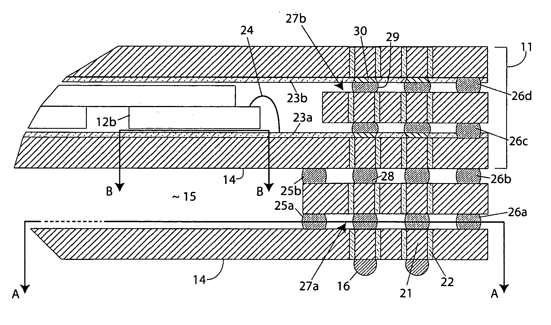
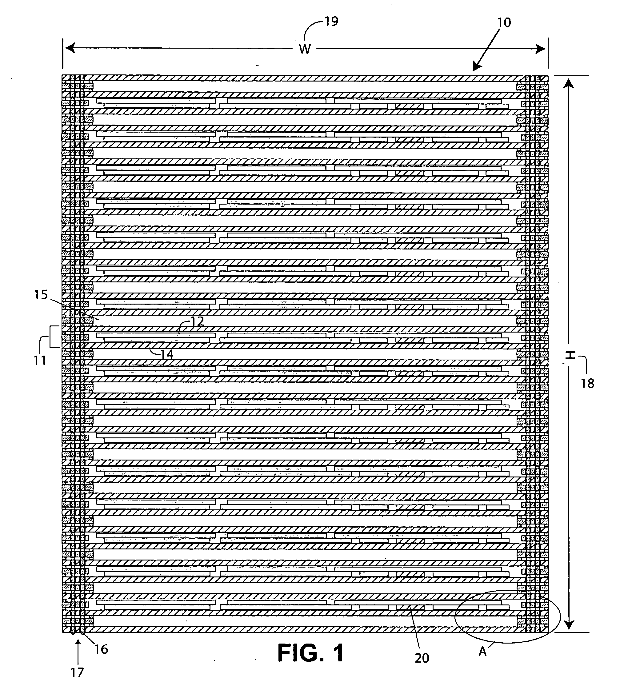
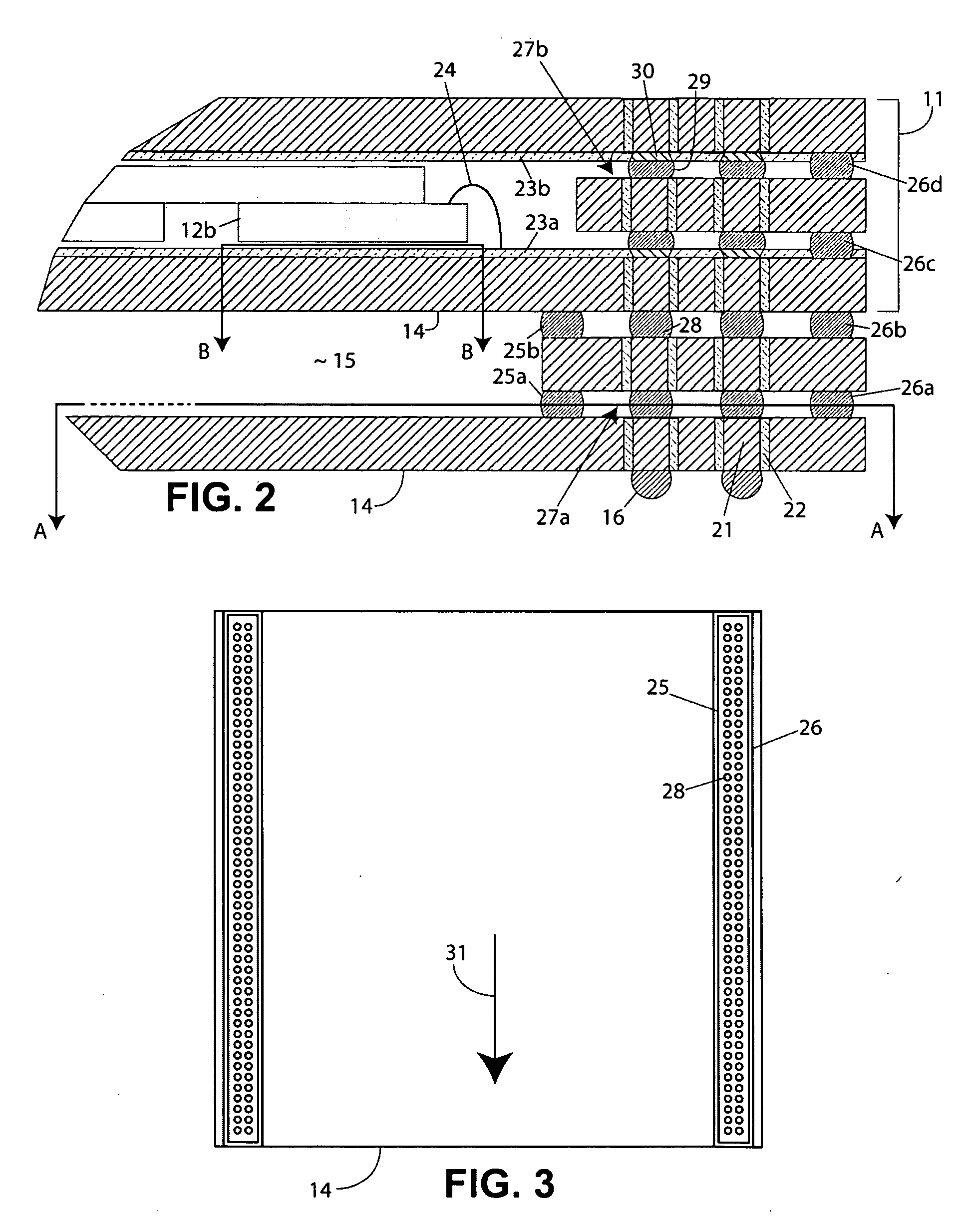
[0026] Various embodiments of the present invention are described hereinafter with reference to the figures. It should be noted that the figures are only intended to facilitate the description of specific embodiments of the invention. They are not intended as an exhaustive description of the invention or as a limitation on the scope of the invention. In addition, an aspect described in conjunction with a particular embodiment of the present invention is not necessarily limited to that embodiment and can be practiced in any other embodiments. For instance, the preferred embodiment describes cooling of the high power laser diodes in the electro-optic chip using heat bumps at the front face of the chip. However, additional cooling may be applied through the back face of the chip, using a thicker chip or a copper slug, as described relative to other circuit elements of the current invention.

[0027] A preferred embodiment of the current invention is a stacked system or subsystem employin...


PUM


Abstract

A flip chip interface is described between a semiconductor chip and a substrate having interconnection circuits. Flip chip bumps are provided at the active face of the chip; each bump is preferably a flexible copper pillar fabricated on a pad, and terminating at the substrate in a well filled with conductive material. The conductive material may be a conductive powder during testing and rework, converting to a melted solder in the final assembly. A mixed array of pillars is provided: signal pillars for signals and power, and more closely spaced heat pillars for conducting heat away from the chip. The signal pillars may be provided in row and column arrays on a background of heat pillars, and the layout of pillars may be adjusted to match local heat patterns in the chip.

Description

[0001] This application claims priority to U.S. provisional patent application Ser. No. 60 / 704,762 filed Aug. 1, 2005, the entire contents of which are hereby incorporated herein by reference.FIELD OF THE INVENTION [0002] This invention relates to electronic packaging, and more particularly to a combination of heat connectors and electrical connectors provided at a flip chip interface between a die and a substrate. DESCRIPTION OF THE RELATED ART [0003] Over the last 40 years transistor density in silicon integrated circuit (IC) chips has increased by a factor greater than 100,000; this phenomenon is known as Moore's Law. Meanwhile, the ability to integrate silicon chips into systems has progressed relatively slowly. Package development can be traced from printed circuit boards (PCBs) having plated through holes (PTHs) around 1970. Surface mount technology (SMT) has followed, also multi-chip modules (MCMs), and systems in package (SIPs). The slow rate of development of integration me...

Claims


Application Information

Patent Timeline
Patent Type & Authority Applications(United States)
IPC IPC(8): H01L23/48
CPCG02B6/4228G02B6/43H01L2924/15311H01L21/486H01L23/49827H01L23/49866H01L25/0657H01L2225/06517H01L2225/0652H01L2225/06541H01L2225/06551H01L2225/06572H01L2225/06582H01L2225/06589H01L2225/06596H01L2924/3011H01L2924/30107H01L2224/48091H01L2224/48227H01L2224/73265H01L2924/00014H01L2224/17107H01L2924/00
Inventor SALMON, PETER C.
Owner SALMON TECH
Why Eureka
Try Eureka