Image sensor with improved light sensitivity

a two-dimensional image and light sensitivity technology, applied in the field of two-dimensional image sensors with improved light sensitivity, can solve the problems of reducing the light sensitivity of each pixel, limiting the speed with which the image is scanned, and image sensors having reduced sensitivity, etc., to achieve short exposure time and broad application

Active Publication Date: 2007-02-01
OMNIVISION TECH INC
View PDF25 Cites 381 Cited by
  • Summary
  • Abstract
  • Description
  • Claims
  • Application Information

AI Technical Summary

Benefits of technology

[0011] Image sensors in accordance with the present invention are particularly suitable for low level lighting conditions, where such low level lighting conditions are the result of low scene lighting, short exposure time, small aperture, or other restriction on light reaching the sensor. They have a broad application and numerous types of image capture devices can effectively use these sensors.

Problems solved by technology

The color filters necessarily reduce the amount of light reaching each pixel, and thereby reduce the light sensitivity of each pixel.
In either case, when color filters are employed the image sensors have reduced sensitivity.
This limits the speed with which the image is scanned and precludes the use of this sensor in a handheld camera or in capturing a scene that includes moving objects.
Although this system improves the light sensitivity over a single conventional image sensor, the overall complexity, size, and cost of the system is greater due to the need for two sensors and a beam splitter.
Furthermore, the beam splitter directs only half the light from the image to each sensor, limiting the improvement in photographic speed.
Increasing gain increases noise as well as signal, causing degradation in the overall signal to noise ratio of the resulting image.

Method used


Image

  • Image sensor with improved light sensitivity
  • Image sensor with improved light sensitivity
  • Image sensor with improved light sensitivity

Examples


Embodiment Construction

[0033] Because digital cameras employing imaging devices and related circuitry for signal capture and correction and for exposure control are well known, the present description will be directed in particular to elements forming part of, or cooperating more directly with, method and apparatus in accordance with the present invention. Elements not specifically shown or described herein are selected from those known in the art. Certain aspects of the embodiments to be described are provided in software. Given the system as shown and described according to the invention in the following materials, software not specifically shown, described or suggested herein that is useful for implementation of the invention is conventional and within the ordinary skill in such arts.

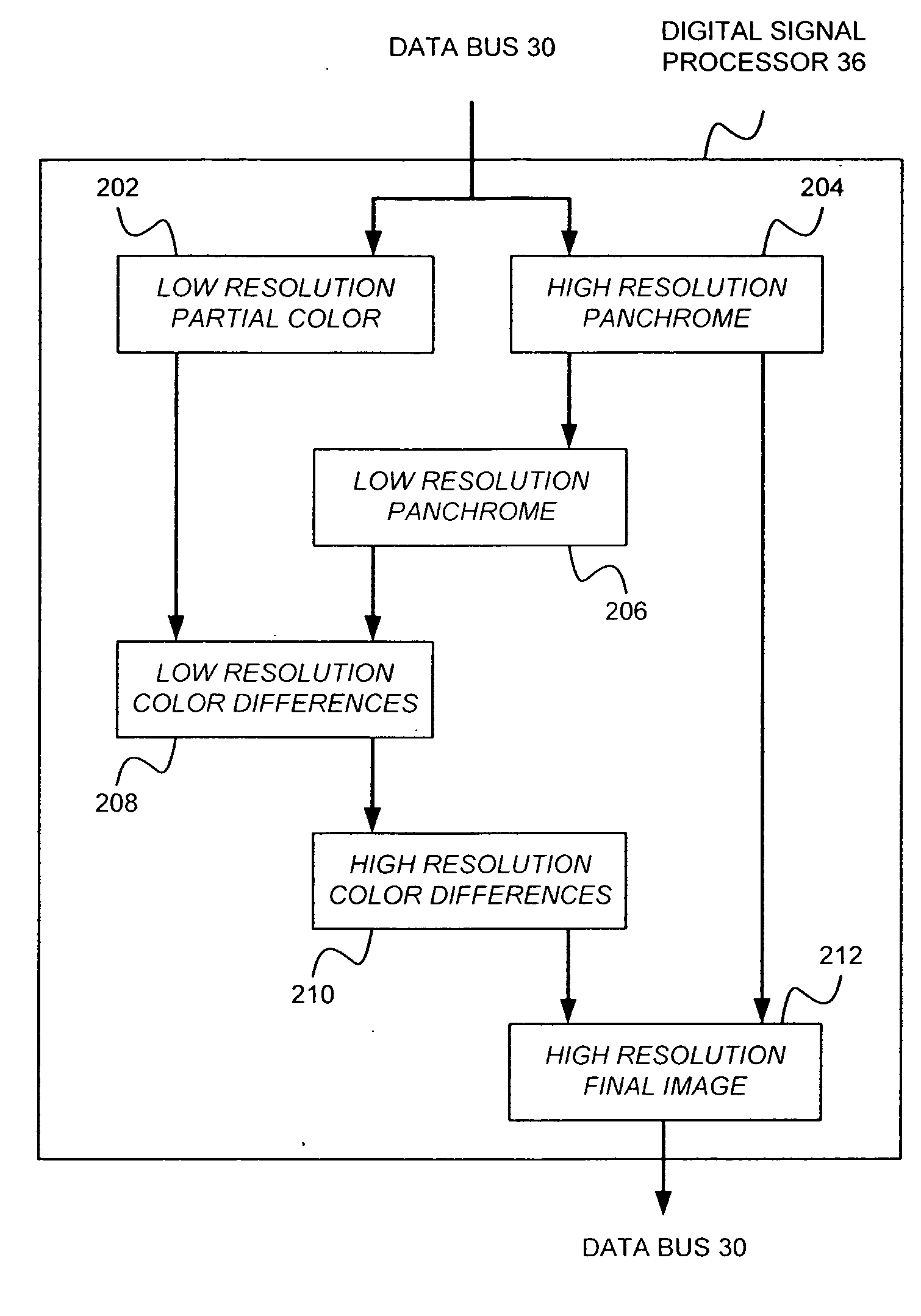
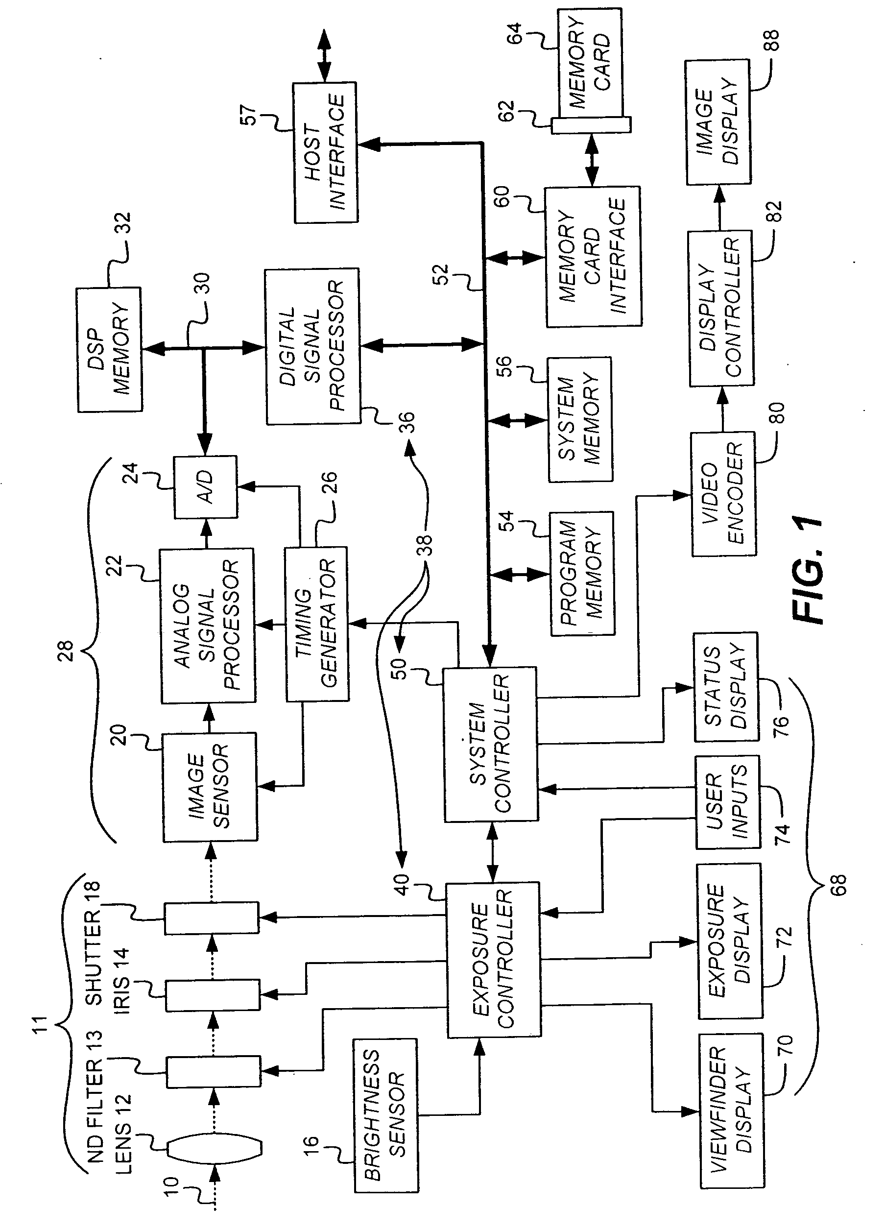
[0034] Turning now to FIG. 1, a block diagram of an image capture device shown as a digital camera embodying the present invention is shown. Although a digital camera will now be explained, the present invention is clearl...


PUM


Abstract

An image sensor for capturing a color image is disclosed having a two-dimensional array having first and second groups of pixels wherein pixels from the first group of pixels have narrower spectral photoresponses than pixels from the second group of pixels and wherein the first group of pixels has individual pixels that have spectral photoresponses that correspond to a set of at least two colors. Further, the placement of the first and second groups of pixels defines a pattern that has a minimal repeating unit including at least twelve pixels. The minimal repeating unit has a plurality of cells wherein each cell has at least two pixels representing a specific color selected from the first group of pixels and a plurality of pixels selected from the second group of pixels arranged to permit the reproduction of a captured color image under different lighting conditions.

Description

CROSS REFERENCE TO RELATED APPLICATIONS [0001] The present application is related to U.S. Serial No. ______, filed concurrently herewith, of John F. Hamilton and John T. Compton, entitled “PROCESSING COLOR AND PANCHROMATIC PIXELS”.FIELD OF THE INVENTION [0002] This invention relates to a two-dimensional image sensor with improved light sensitivity BACKGROUND OF THE INVENTION [0003] An electronic imaging system depends on an electronic image sensor to create an electronic representation of a visual image. Examples of such electronic image sensors include charge coupled device (CCD) image sensors and active pixel sensor (APS) devices (APS devices are often referred to as CMOS sensors because of the ability to fabricate them in a Complementary Metal Oxide Semiconductor process). Typically, these images sensors include a number of light sensitive pixels, often arranged in a regular pattern of rows and columns. For capturing color images, a pattern of filters is typically fabricated on t...

Claims


Application Information

Patent Timeline
Patent Type & Authority Applications(United States)
IPC IPC(8): H04N1/46
CPCH04N9/045H04N23/633H04N23/843H04N25/133H04N25/136H04N25/134
Inventor COMPTON, JOHN T.HAMILTON, JOHN F. JR.
Owner OMNIVISION TECH INC
Why Eureka
Try Eureka