Method of fabricating Ge or SiGe/Si waveguide or photonic crystal structures by selective growth

a selective growth and waveguide technology, applied in the direction of optical waveguide light guide, instruments, etc., can solve the problems of large scattering loss, 10 db/cm, scattering loss, etc., to improve crystal quality, improve crystal quality, and reduce scattering loss

Active Publication Date: 2007-02-01
MASSACHUSETTS INST OF TECH
View PDF1 Cites 80 Cited by
  • Summary
  • Abstract
  • Description
  • Claims
  • Application Information

AI Technical Summary

Benefits of technology

[0007] According to one aspect of the invention, there is provided a low loss crystal quality waveguide. The waveguide includes a substrate and a dielectric layer that is formed on the substrate. A channel is formed by etching a portion of the dielectric layer. A selective growth of a Si, Ge, or SiGe layer is performed in the area that defines the channel. The waveguide is annealed at a defined temperature range to improve the crystal quality.
[0008] According to another aspect of the invention, there is provided a photonic crystal structure. The photonic structure includes a substrate and a dielectric layer that is formed on the substrate. An array of holes are formed by etching a portion of the dielectric layer. A selective growth of a Si, Ge, or SiGe layer is performed in these holes. The photonic crystal structure is annealed at a defined temperature range to improve the crystal quality.
[0009] According to another aspect of the invention, there is provided a method of fo

Problems solved by technology

One of the challenges from etching is the formation of rough sidewalls which causes scattering loss.
For high index contrast waveguides with dimensions close to or less than the propagation wavelength in the core materials, there is a large amount of scattering loss (>10 dB/cm) and this becomes more of a challenge with the decrease of dimensions used in waveguides.
This becomes a very serious problem for Ge based waveguide since Ge's refractive index is among the highest (˜4.0) which require much smaller size than conventional materials such as Si waveguide.
The roughness inevitably introduces more loss when the l

Method used


Image

  • Method of fabricating Ge or SiGe/Si waveguide or photonic crystal structures by selective growth
  • Method of fabricating Ge or SiGe/Si waveguide or photonic crystal structures by selective growth
  • Method of fabricating Ge or SiGe/Si waveguide or photonic crystal structures by selective growth

Examples


Embodiment Construction

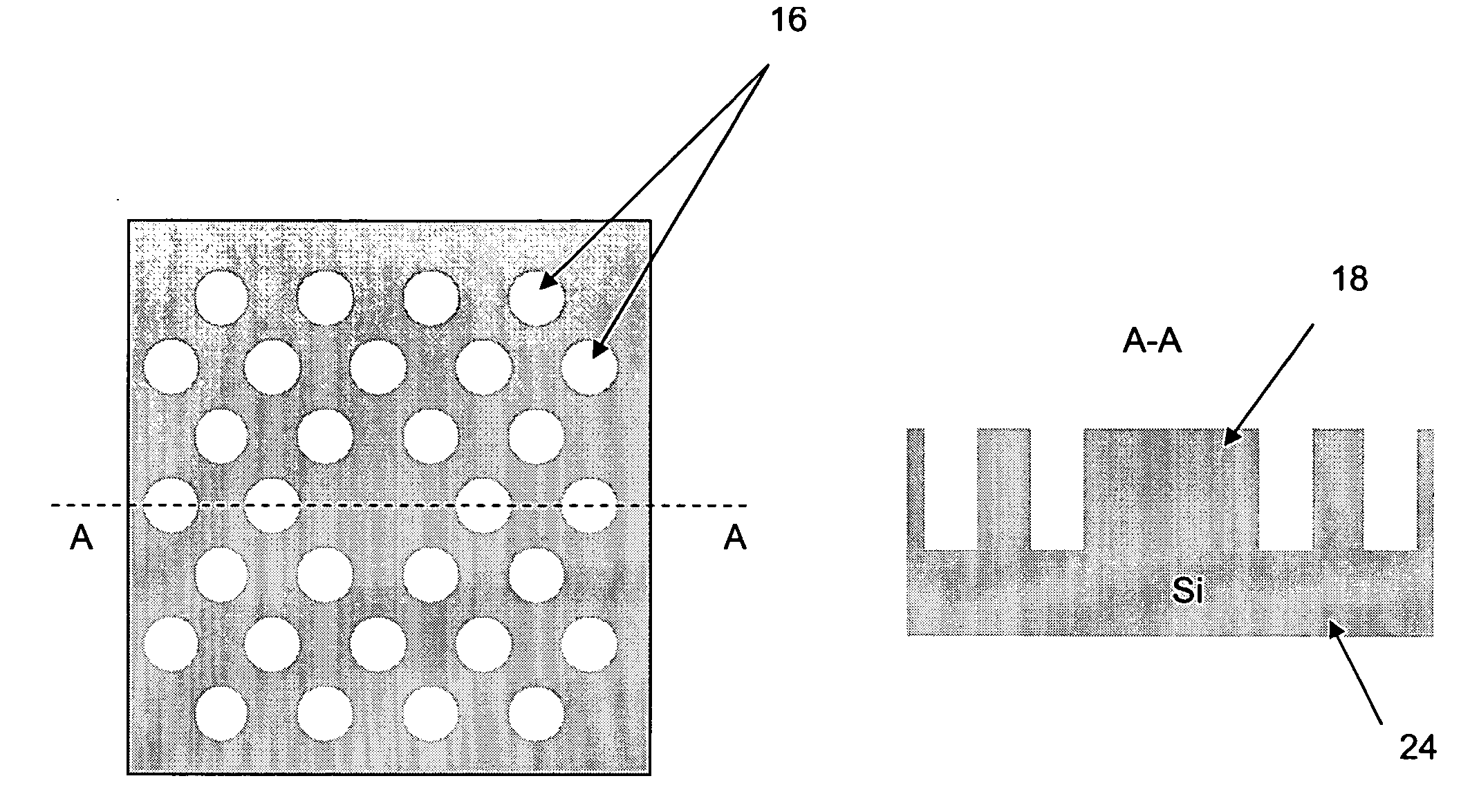
[0016] The invention involves an inventive technique to make low loss crystal quality waveguides by selective growth, where there is no sidewall scattering loss from etching. The core idea is to grow a Si, Ge or SiGe waveguide directly on a small Si area surrounded by SiO2, since Ge or SiGe cannot grow on the top of SiO2.

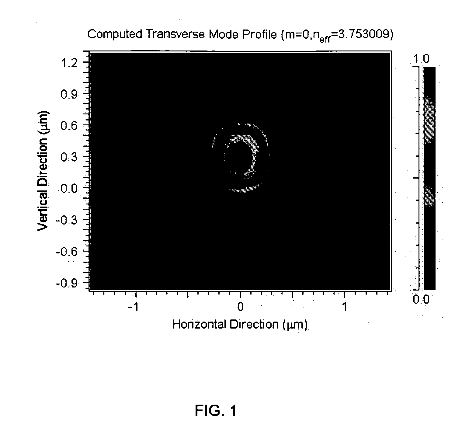
[0017]FIG. 1 shows the mode profile of a waveguide structure having dimensions less than the propagation wavelength in the core material (in this case λ=1.55 cm). At this dimension, the scattering of light due to side wall roughness becomes very significant. This illustrates the constraints being faced and how difficult to attend waveguide structure to operate efficiently at those ranges.

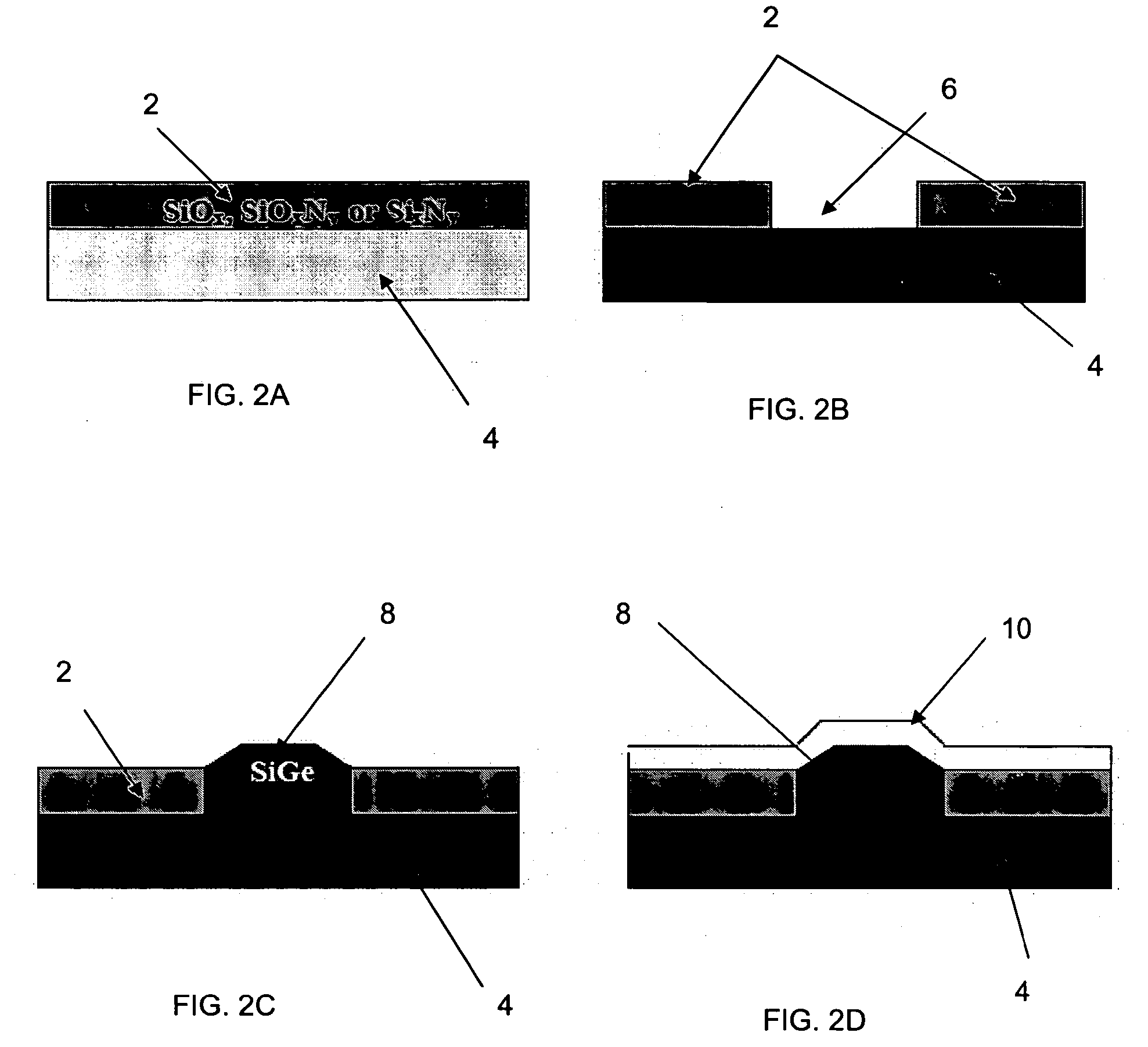
[0018]FIGS. 2A-2D are schematic diagrams illustrating the steps followed according to the invention. A Si substrate 4 is provided and a SiO2 layer 2 is either formed or deposited on the Si substrate 4, as shown in FIG. 2A. Note other materials beside SiO2 can also be used in accor...


PUM


Abstract

A method of forming a low loss crystal quality waveguide is provided. The method includes providing a substrate and forming a dielectric layer on the substrate. A channel is formed by etching a portion of the dielectric layer. A selective growth of a Si Ge, or SiGe layer is performed in the area that defines the channel. Furthermore, the method includes thermally annealing the waveguide at a defined temperature range.

Description

BACKGROUND OF THE INVENTION [0001] The invention relates to the field of Ge or SiGe waveguides for integrated optical circuits and far infrared application, and in particular to making low loss crystal quality waveguides and photonic crystal structures where there is no sidewall scattering loss from etching. [0002] The waveguide structures often referred to when fabricating Ge or SiGe / Si waveguides are two structures: channel waveguides and ridge waveguides. These waveguide structures also come with the shape of bend, ring, microdisk or taper. One exemplary way to make them includes the deposition of one higher index material (core) whose the refractive index is higher than surrounding materials, and then etching the material into the channel (deep etch) or ridge (shallow etch) structure followed by a deposition of surrounding materials. For example, a semiconductor laser generally has a ridge waveguide structure. [0003] The etching process usually defines the dimension of the waveg...

Claims


Application Information

Patent Timeline
IPC IPC(8): G02B6/10
CPCB82Y20/00G02B6/1223G02B2006/12169G02B6/131G02B6/136G02B6/1225
Inventor PAN, DONGLIU, JIFENGMICHEL, JURGENYASAITIS, JOHNKIMERLING, LIONEL C.
Owner MASSACHUSETTS INST OF TECH
Why Eureka
Try Eureka