Semiconductor device for protecting rechargeable battery

a technology of a semiconductor device and a rechargeable battery, which is applied in the direction of safety/protection circuits, emergency protective circuit arrangements, transportation and packaging, etc., can solve the problems of reducing and affecting the operation efficiency of the load regulator. achieve the effect of not increasing the area size of the ic chip

Active Publication Date: 2007-02-08
NISSHINBO MICRO DEVICES INC
View PDF3 Cites 7 Cited by
  • Summary
  • Abstract
  • Description
  • Claims
  • Application Information

AI Technical Summary

Benefits of technology

[0013] The present invention was conceived in view of the above-described problems, and the invention may provide a semiconductor device for protecting a rechargeable cell that can deal with different levels of excessive discharge currents without increasing the area size of the IC chip.

Problems solved by technology

Because the amount of energy held inside a high-capacity battery cell is very large, intense heat is likely to be produced by overcharge, over discharge or overcurrent, which intense heat may causes fire.
However, if the circuit is designed so as to be switched off right after the detection signal is output, electric supply to the load regulator may be stopped by a very short pulse (such as noise) that is perceived as the detection signal.
This results in error operations.
These delay times, however, cause inspection time to be increased in characteristic inspection or shipping inspection of the protection IC, and lead to fall of mass productivity and increase of the cost.
Addition of a single pin of the test terminal may cause the package to be replaced with a larger-size package, or cause the number of bonding pads of the test terminal to increase.
As a result, the IC chip size, the required space, and the cost increase.
This arrangement inevitably causes the area size of the IC chip and the cost to be increased.

Method used


Image

  • Semiconductor device for protecting rechargeable battery
  • Semiconductor device for protecting rechargeable battery
  • Semiconductor device for protecting rechargeable battery

Examples


Embodiment Construction

[0033] The preferred embodiment of the present invention is described below in conjunction with the attached drawings. The components described in the embodiment, types, combinations, shapes and the positional relationship thereof are used only for the exemplified purpose, and the invention is not limited to these examples.

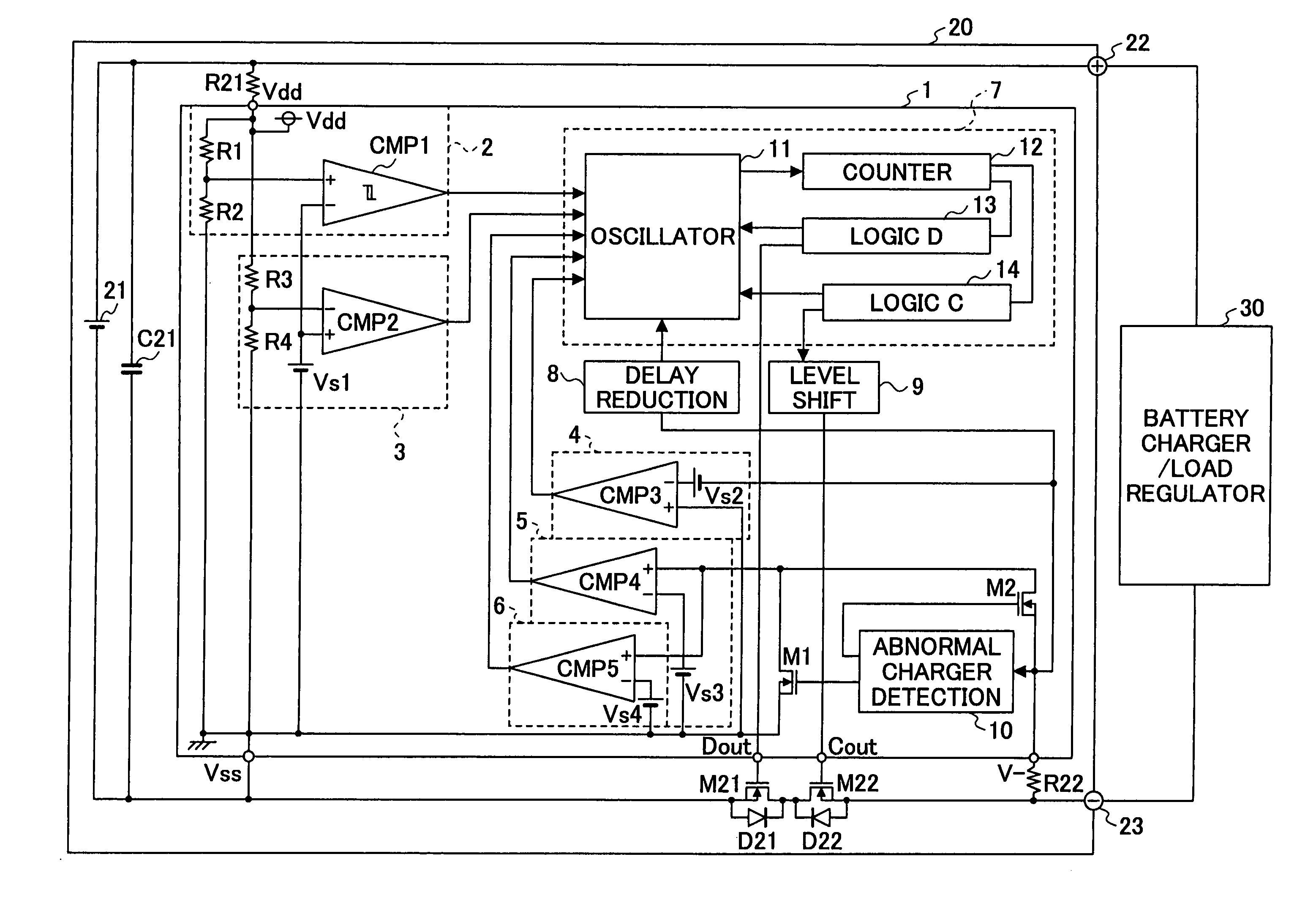
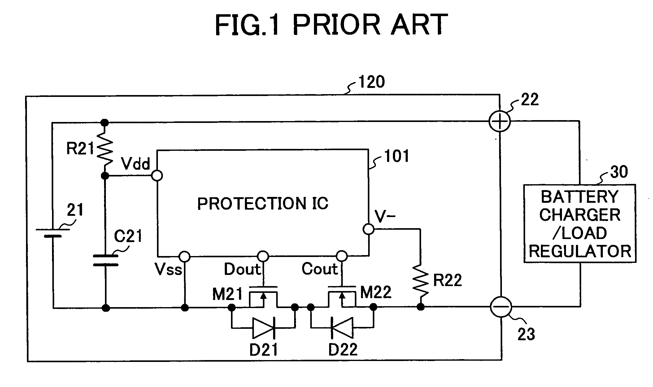
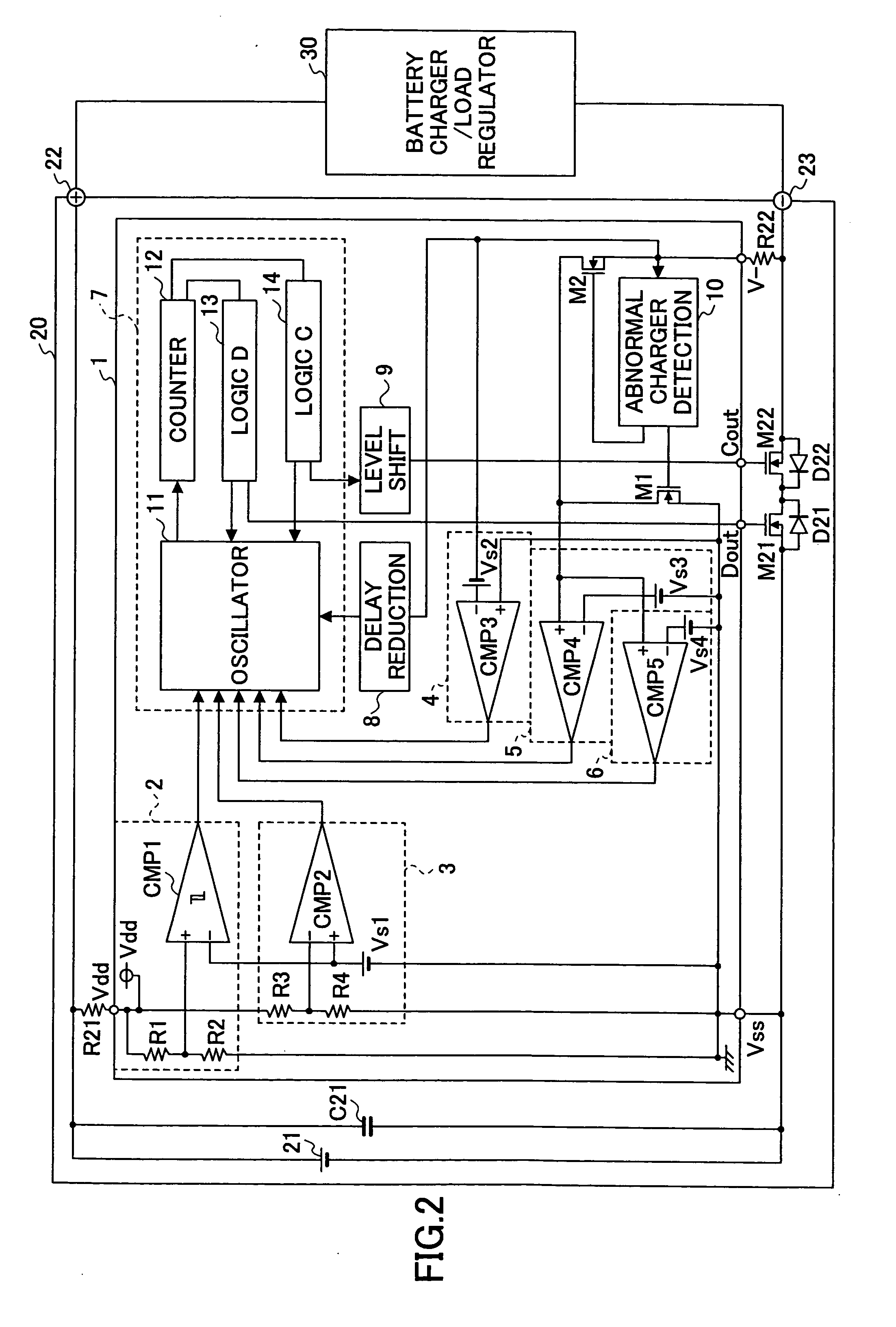
[0034]FIG. 2 is a circuit diagram of a battery pack according to an embodiment of the invention. The battery pack 20 includes a protection IC (or a semiconductor device for rechargeable cell protection) 1, a rechargeable (secondary) cell 21, a discharge-control NMOS transistor M21, a charging-control NMOS transistor M22, a capacitor C21, and resistors R21 and R22. The battery pack 20 also has a positive terminal 22 and a negative terminal 23, which terminals are electrically connected to a battery charger or load regulator 30.

[0035] The protection IC 1 includes an overcharge detection circuit 2, an over discharge detection circuit 3, an excessive charging curren...


PUM


Abstract

A semiconductor device for protecting a rechargeable cell at least from excessive discharge current due to over discharge of the rechargeable cell, includes (a) a first excessive discharge current detection circuit configured to detect first excess of a voltage at an externally or an internally provided electric current detection terminal exceeding a first voltage level (Vs3), (b) a second excessive discharge current detection circuit configured to detect second excess of the absolute voltage at the electric current detection terminal exceeding a second voltage level (Vs4) higher than the first voltage level, (c) a delay circuit configured to cause each of the first and second excessive discharge current detection circuits to delay its output by a predetermined delay time, and (d) a delay reducing circuit configured to produce a delay time reducing signal for reducing the delay time at a predetermined ratio when a negative voltage lower than a predetermined negative voltage level or a positive voltage higher than a third voltage level (Vt) is applied to the electric current detection terminal.

Description

BACKGROUND OF THE INVENTION [0001] 1. Field of the Invention [0002] The present invention relates to a semiconductor device for protecting a rechargeable battery, and more particularly, to a protection IC for protecting a lithium-ion cell accommodated in a rechargeable battery pack used for portable electronic devices from overcharge, over discharge, excessive charging or discharge current, or short-circuit current. [0003] 2. Description of Related Art [0004] Conventionally, easy-handling battery packs have been in widespread use for power sources of portable electronic devices. A battery pack is comprised of one or more secondary (rechargeable) cells accommodated in a package. Secondary cells are in general high-capacity battery cells, such as lithium-ion cells, lithium polymer batteries, or nickel hydride batteries. Because the amount of energy held inside a high-capacity battery cell is very large, intense heat is likely to be produced by overcharge, over discharge or overcurrent...

Claims


Application Information

Patent Timeline
Patent Type & Authority Applications(United States)
IPC IPC(8): H02H3/24
CPCH02H7/18H02J2007/004H02J7/0031H02J7/00306
Inventor YANO, KOICHIFUJIWARA, AKIHIKO
Owner NISSHINBO MICRO DEVICES INC
Why Eureka
Try Eureka