Chemical vapor deposition chamber with dual frequency bias and method for manufacturing a photomask using the same

Inactive Publication Date: 2007-02-08
APPLIED MATERIALS INC
View PDF21 Cites 68 Cited by
  • Summary
  • Abstract
  • Description
  • Claims
  • Application Information

AI Technical Summary

Problems solved by technology

Thus, any defects in the mask may be transferred to the chip, potentially adversely affecting performance.
Defects that are severe enough may render the mask completely useless.
As the photoresist is slightly etched during the etching process, dimensional control of the critical dimensions of the photomask layers being etched suffers.
However, as critical dimensions, particularly of the photomask itself, are reduced below about 5 μm and into the nanometer regime, edge roughness of photoresist apertures is of a magnitude equal to that of the critical dimension itself, and thus, even slight variation is roughness may cause the critical dimensions to become out of specification.
Moreover, si

Method used


Image

  • Chemical vapor deposition chamber with dual frequency bias and method for manufacturing a photomask using the same
  • Chemical vapor deposition chamber with dual frequency bias and method for manufacturing a photomask using the same
  • Chemical vapor deposition chamber with dual frequency bias and method for manufacturing a photomask using the same

Examples


Embodiment Construction

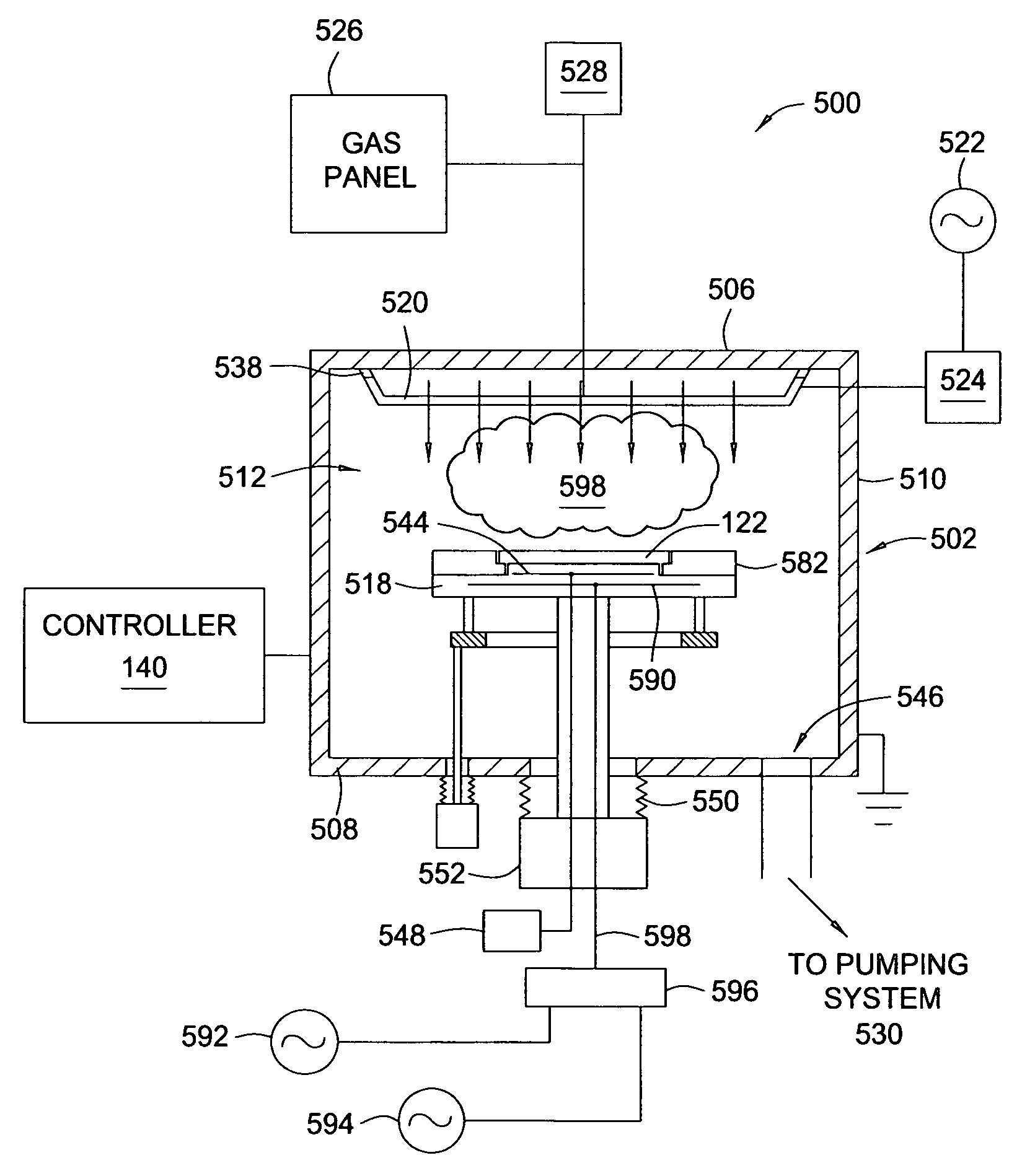
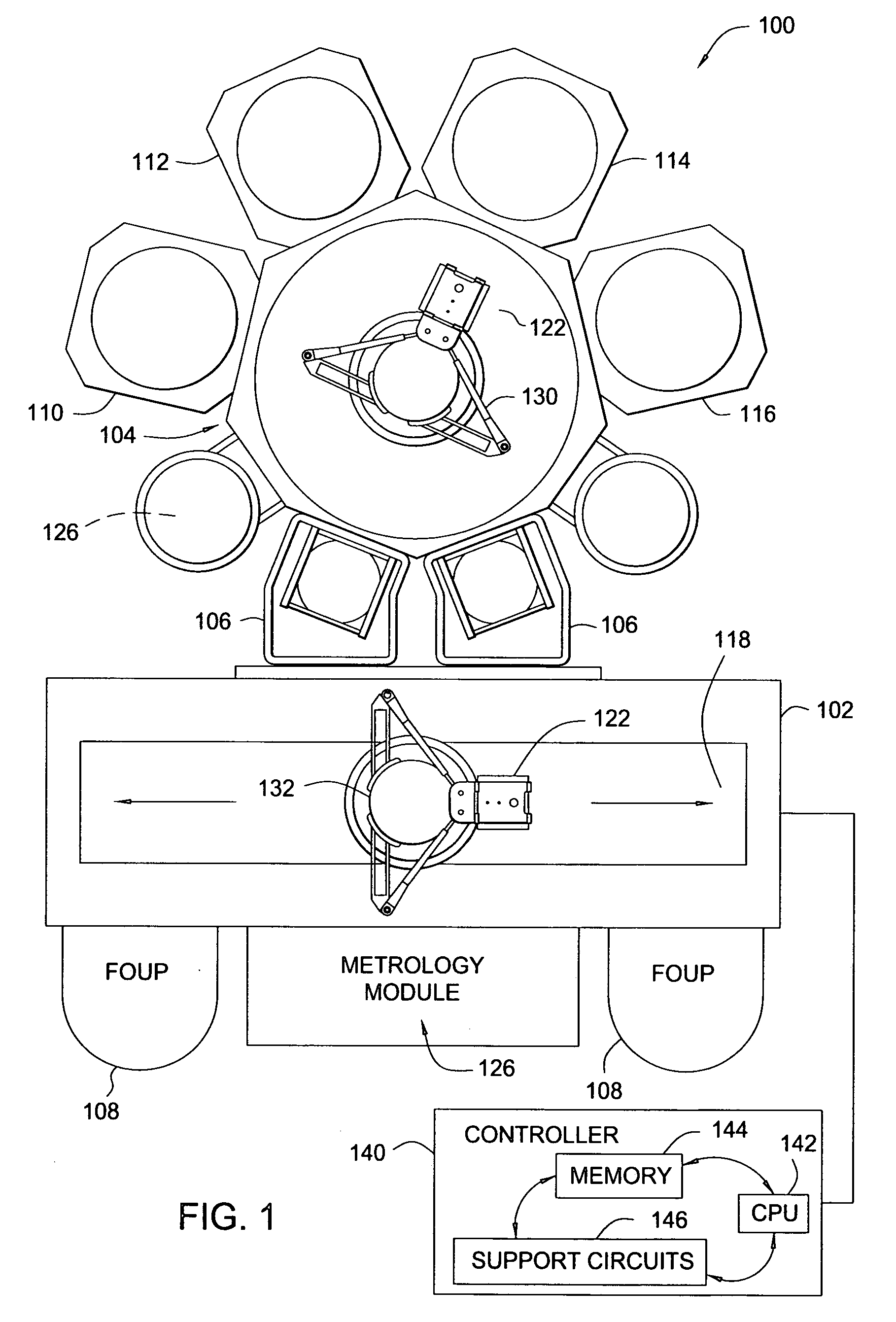
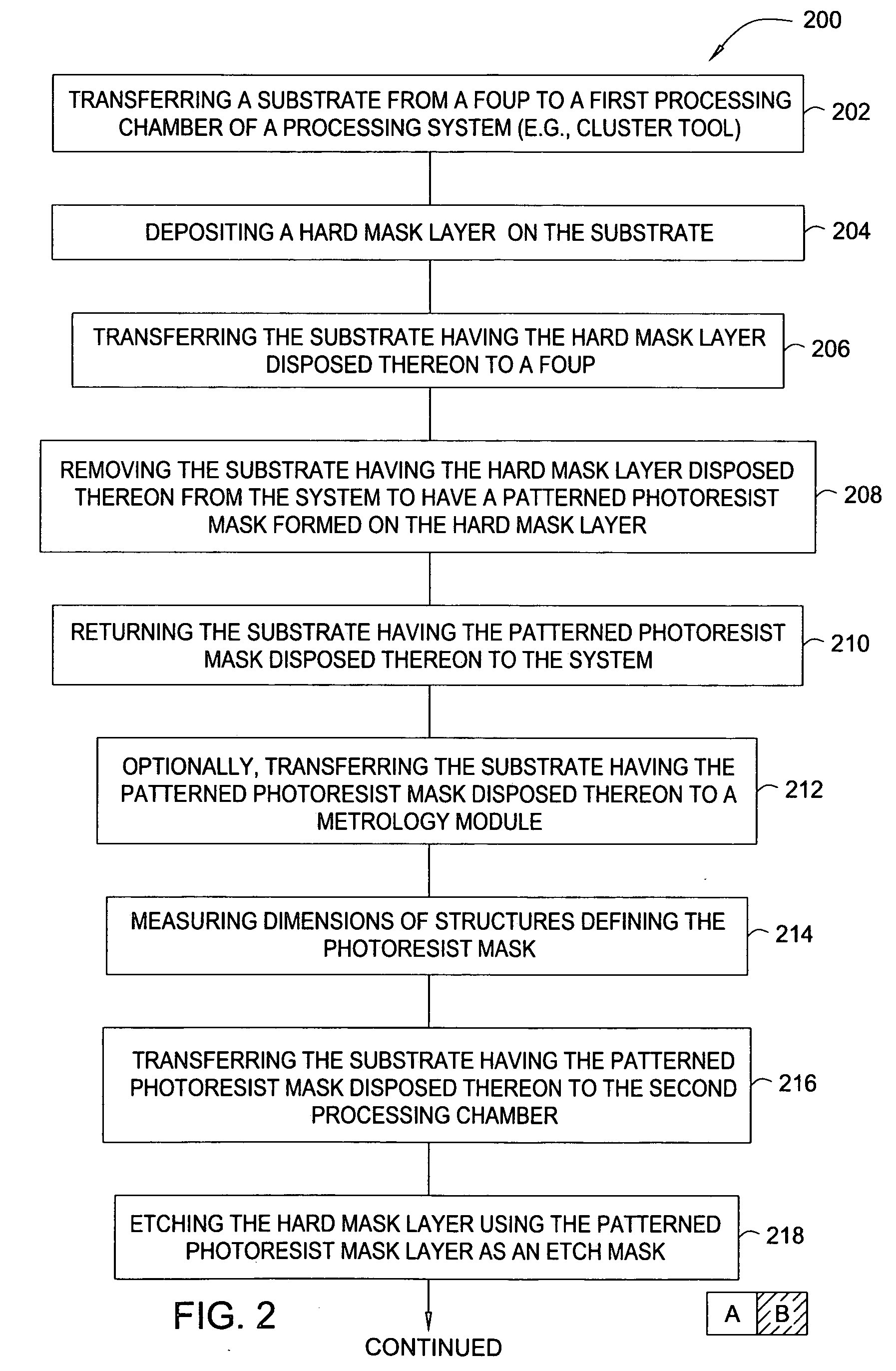
[0025] Embodiments of the present invention include an improved process for photomask fabrication, and an improved cluster tool and method for process integration in manufacture of photomasks. The photomask fabrication method includes forming an ultra-thin hard mask upon a film stack that is processed into a photomask. The film stack generally includes a chromium containing layer and a quartz layer. The film stack may additionally include a light-attenuating layer, such as a layer containing molybdenum. In one embodiment, the hard mask material may be chosen from a material having a high selectivity to the underlying layer being etched, such as quartz and / or chromium containing layers. In another embodiment, the hard mask material may be chosen from a material having an etch rate comparable to that of the underlying layer to be etched through the hard mask. As the hard masks of the present invention are not laterally etched using the chemistries described herein, dimensional stabili...


PUM

PropertyMeasurementUnit
Poweraaaaaaaaaa
Volumeaaaaaaaaaa
Frequencyaaaaaaaaaa

Abstract

A method and apparatus for process integration in manufacture of a photomask are disclosed. In one embodiment, a cluster tool suitable for process integration in manufacture of a photomask including a vacuum transfer chamber having coupled thereto at least one hard mask deposition chamber and at least one plasma chamber configured for etching chromium. In another embodiment, a method for process integration in manufacture of a photomask includes depositing a hard mask on a substrate in a first processing chamber, depositing a resist layer on the substrate, patterning the resist layer, etching the hard mask through apertures formed in the patterned resist layer in a second chamber; and etching a chromium layer through apertures formed in the hard mask in a third chamber.

Description

BACKGROUND OF THE INVENTION [0001] 1. Field of the Invention [0002] The present invention generally relates to a method for photomask fabrication using a hard mask, and to a cluster tool and method for process integration in manufacturing of a photomask. [0003] 2. Description of the Related Art [0004] In the manufacture of integrated circuits (IC), or chips, patterns representing different layers of the chip are created by a chip designer. A series of reusable masks, or photomasks, are created from these patterns in order to transfer the design of each chip layer onto a semiconductor substrate during the manufacturing process. Mask pattern generation systems use precision lasers or electron beams to image the design of each layer of the chip onto a respective mask. The masks are then used much like photographic negatives to transfer the circuit patterns for each layer onto a semiconductor substrate. These layers are built up using a sequence of processes and translate into the tiny ...

Claims


Application Information

Patent Timeline
IPC IPC(8): C23C16/00C23C14/00B05C5/00B05D3/00
CPCC23C16/509C23C16/56H01J37/32082H01L21/67207H01J37/32357H01J37/32706H01L21/67069H01J37/321C23C16/4585G03F1/26
Inventor KUMARGREWAL, VIRINDERYAU, WAI-FAN
Owner APPLIED MATERIALS INC
Why Eureka
Try Eureka