Inductance analysis system and method and program therefor

a technology of inductance analysis and analysis method, applied in the direction of detecting faulty computer hardware, error detection/correction, instruments, etc., can solve the problems of limited application, insufficient analysis time, and insufficient analysis time, and achieve the effect of high accuracy at a large scale and short tim

a technology of inductance analysis and analysis method, applied in the direction of detecting faulty computer hardware, error detection/correction, instruments, etc., can solve the problems of limited application, insufficient analysis time, and insufficient analysis time, and achieve the effect of high accuracy at a large scale and short tim

US20070033553A1Inactive Publication Date: 2007-02-08LONGITUDE SEMICON S A R L

Image

  • Inductance analysis system and method and program therefor
  • Inductance analysis system and method and program therefor
  • Inductance analysis system and method and program therefor

Examples


Embodiment Construction

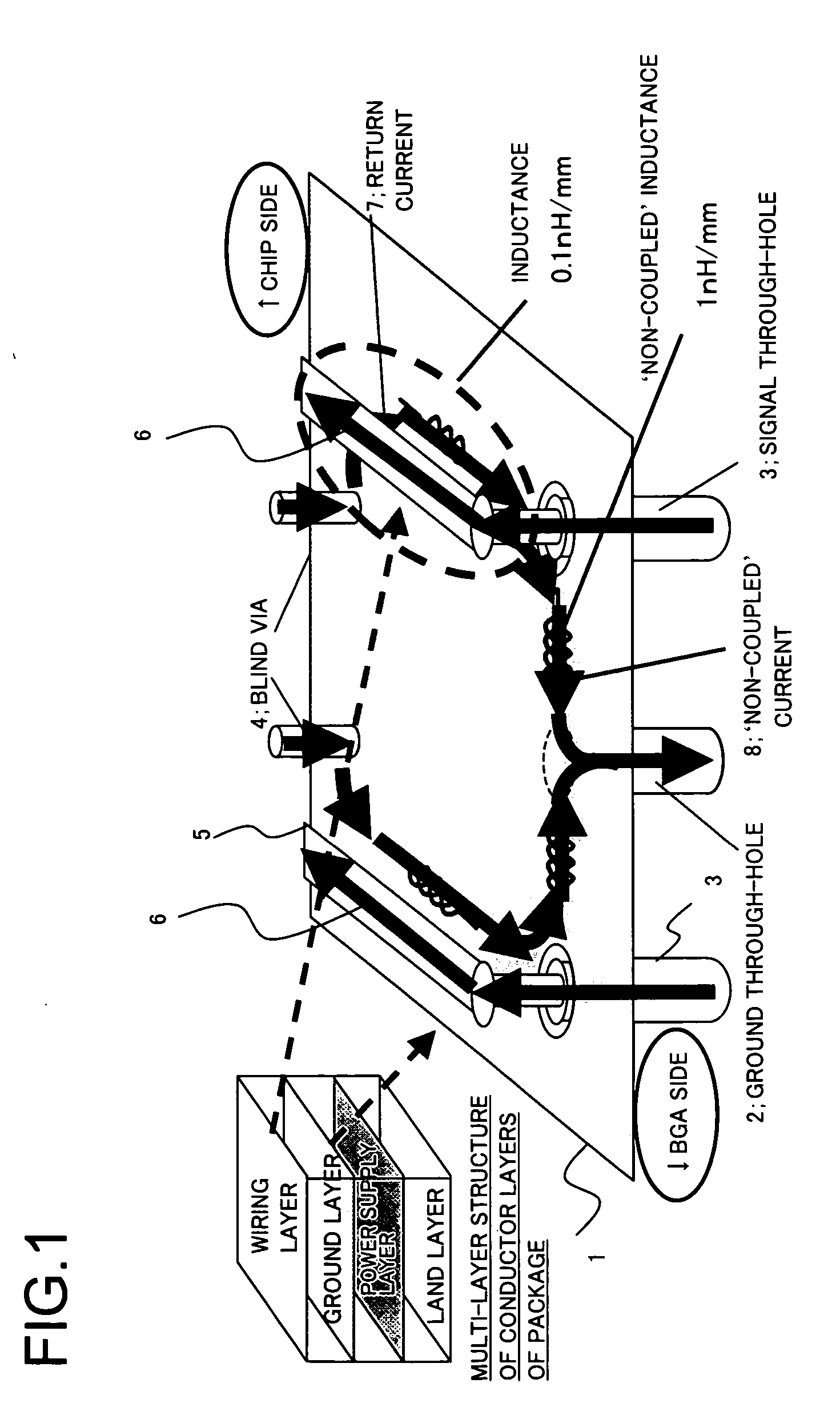
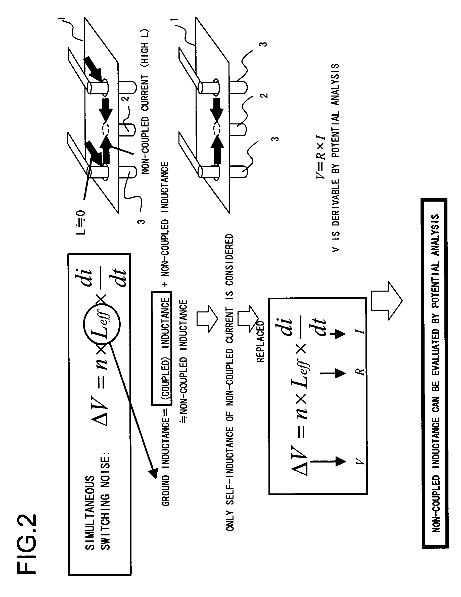
[0034] The present invention will now be described in detail with reference to the drawings. Referring to FIG. 1, signal through-holes 3 are passed through a ground plane 1. To this ground plane 1 are connected a ground through-hole 2 and blind vias 4. When signal current 6 flows through a signal wire 5 in a wiring layer, return current 7 flows on the ground plane 1 in a direction opposite to the direction along which flows the signal current 6. Due to a coupling electromagnetic field, the return current 7 flows through an area lying directly below the signal wire 6. However, the return current is not coupled to an electromagnetic field of non-coupled current 8 proceeding towards the ground through-hole 2, and hence the inductance (non-coupled inductance) is increased. That is, if there flows much non-coupled current, the ground inductance is increased. There are occasions where, for example, the non-coupled inductance is as high as 1 nH / mm for the coupled inductance of 0.1 nH / mm. T...


PUM


Abstract

System, method and program for inductance analysis for reducing time for analysis, to cope with increase in the system size, to achieve high accuracy in the analysis. Information on a power supply plane, in a state in which a beginning point of non-coupled current of return current accompanying a signal current is placed in the vicinity of a signal through-hole on the power supply plane, based on position information of said signal through-hole, is received. Potential distribution in the power supply plane is determined and output. The non-coupled inductance from the signal through-hole to the power supply through-hole in the power supply plane is evaluated. In the potential analysis, non-coupled inductance L from the signal through-hole to the power supply through-hole is represented by resistance R. The relationship that a voltage increment ΔV is represented by the product of the non-coupled inductance L and the rate of time change of the current, ΔV=LΔI / Δt, is replaced by the relationship that the voltage V is represented by the product of resistance R and non-coupled current I, V=R×I. Potential analysis is performed by analyzing two-dimensional heat diffusion in the power supply plane assuming that a heat source is placed at a beginning point of the non-coupled current.

Description

FIELD OF THE INVENTION [0001] This invention relates to a technology for designing and manufacture of semiconductor devices. More particularly, this invention relates to a system, a method and a program for analysis convenient for e.g. a semiconductor package board. BACKGROUND OF THE INVENTION [0002] A package board, including a core layer and built-up layers and carrying a semiconductor chip and a BGA (ball grid array) terminal on its one major surface and on its opposite major surface, respectively, with an electrode of the semiconductor chip being extended to the BGA surface, has been in extensive use, because the power supply and the ground are provided as planes or layers, with the inductance and the noise being small. However, with increase in the operating frequency of the LSIs in these days, the power supply noise and the ground noise have increased. In particular, the simultaneous switching noise has become of a serious problem. [0003] Reference will now be made to FIG. 6. ...

Claims


Application Information

Patent Timeline
08 Feb 2007
Publication
US20070033553A1
IPC
G06F17/50
CPC
G06F17/5036; H05K3/0005; H05K1/115; G06F30/367
Inventors
KATAGIRI, MITSUAKI; IIDA, TAKASHI