Integrated RF circuits

a technology of integrated circuits and frequency bands, applied in the field of radiofrequency (rf) integrated circuits, can solve the problems of vector error in modulation methods, production yield problems, overall performance, etc., and achieve the effect of reducing the design process, small die area, and large response tuning rang

Inactive Publication Date: 2007-02-15
NOKIA CORP
View PDF0 Cites 28 Cited by
  • Summary
  • Abstract
  • Description
  • Claims
  • Application Information

AI Technical Summary

Benefits of technology

[0016] Advantages of the adjuster according to the second aspect of the invention include adaptivity and extremely large response tuning range especially in phase, 0 . . . 360 degrees; relatively small die area; and design process is alleviated, since phase tuning phase must not be considered.

Problems solved by technology

The uncontrollable signal response behavior (phase & amplitude) of the electrical devices caused by process variations and mismatches in general integrated circuit processes cause various unwanted features in the overall performance.
These kinds of circuit structures are, for instance, traditional radio frequency linearization and modulation correction circuitries, in which the uncontrollable signal response behavior cause vector error in modulation methods or inaccuracy in linearization or feedback loops.
This approach further suffers from many inaccuracies especially mismatch of active elements and the external interfaces like packaging and bonding, which cause production yield problems.
Also the electrical length has a significant frequency limitation, which has forced to utilize different kind of control mechanism.
Furthermore, a phase shift realized by an external strip line is frequency selective and will deteriorate the wideband operation of the linearization.
In addition, the component mismatches cause an error in the quality of the modulation.
However, these implementations have remained in laboratory phase without commercial products.

Method used


Image

  • Integrated RF circuits
  • Integrated RF circuits
  • Integrated RF circuits

Examples


example embodiments

DESCRIPTION OF EXAMPLE EMBODIMENTS

First Aspect of the Invention

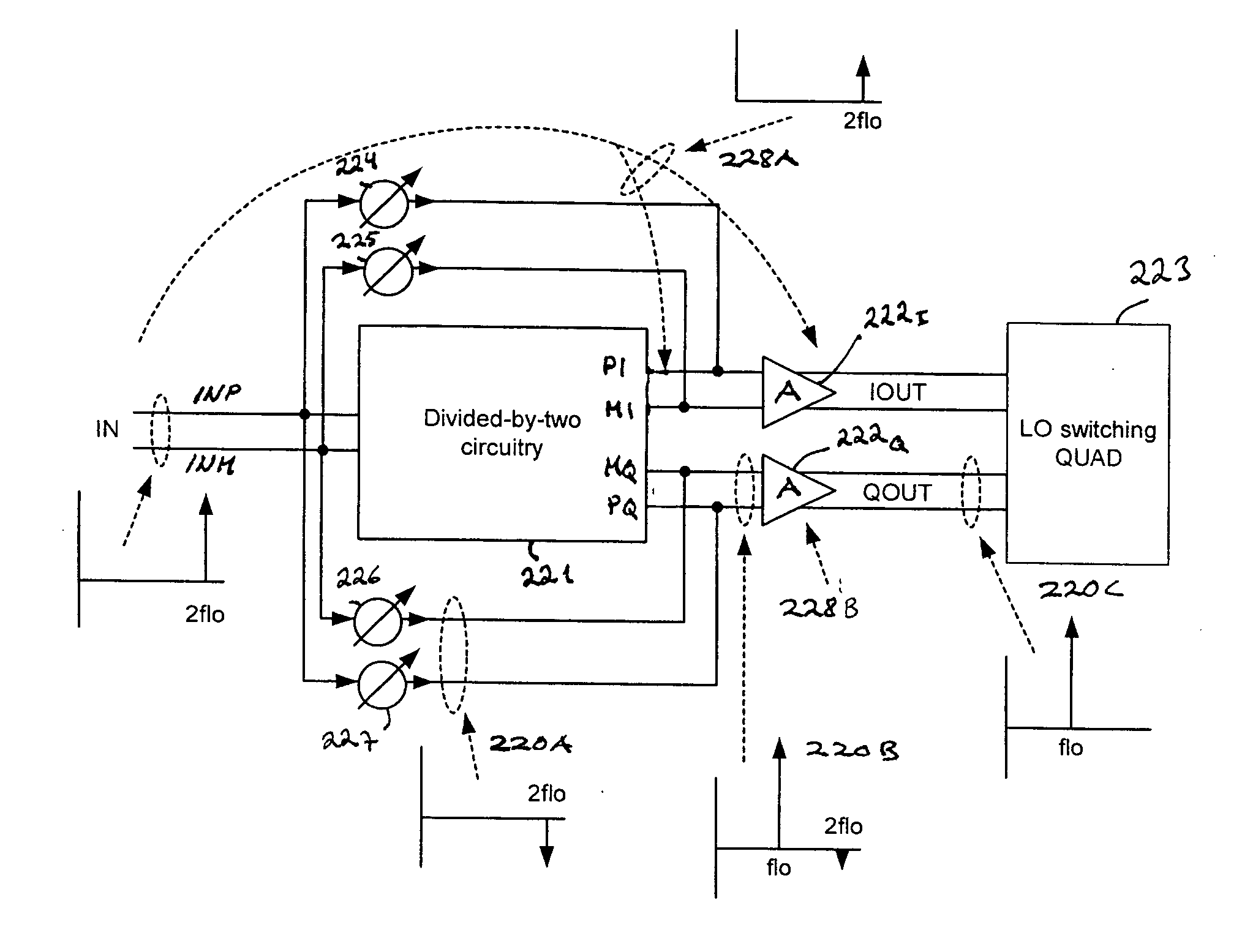
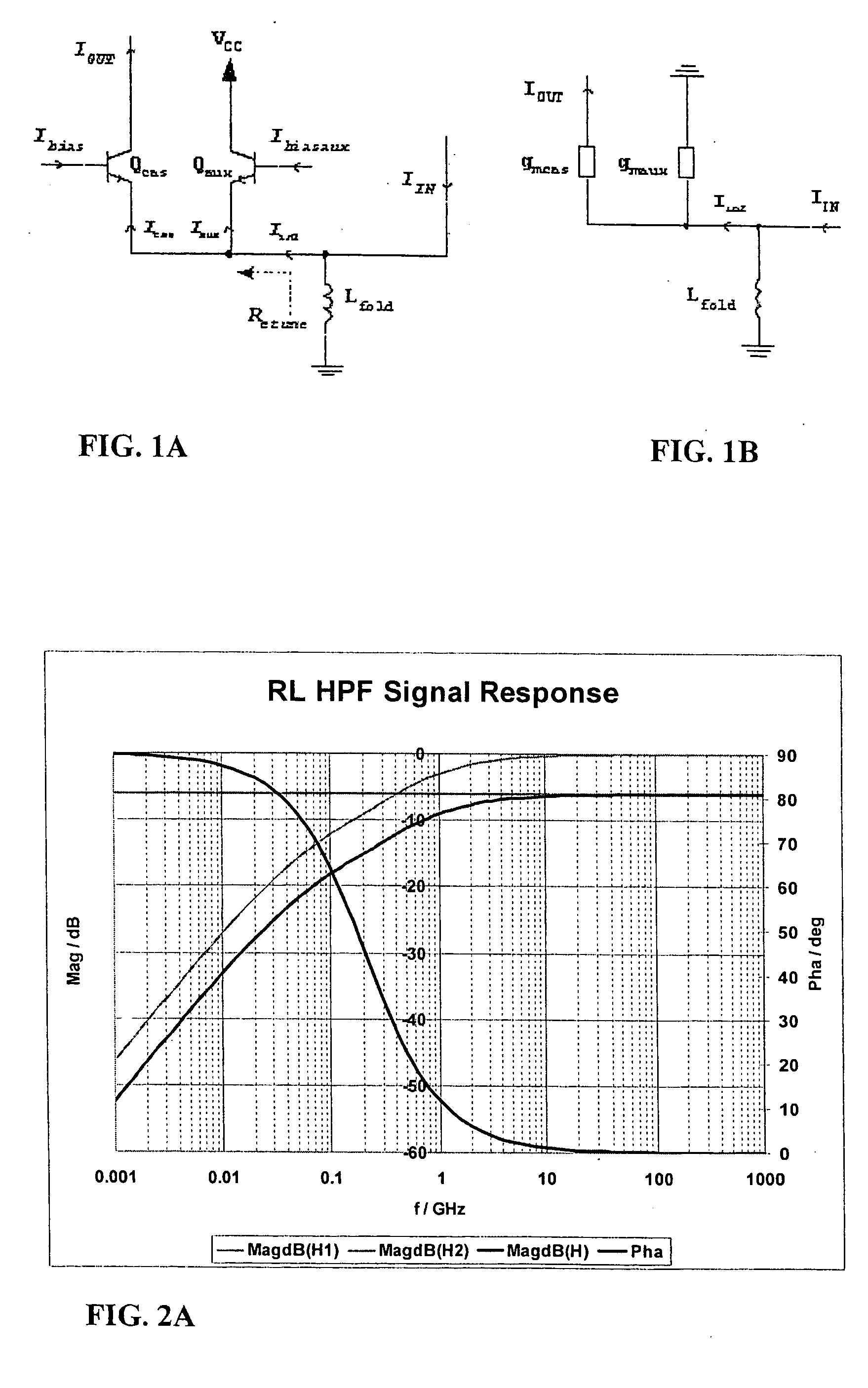
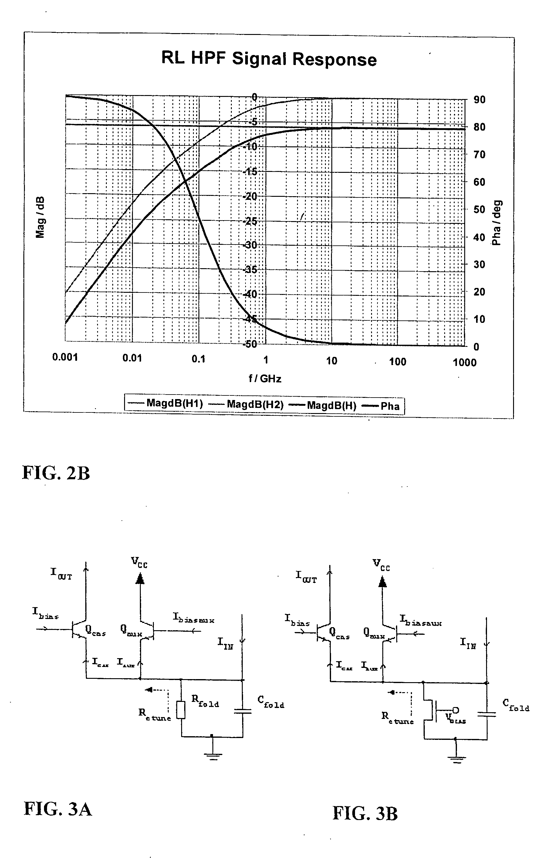
[0044] Examples of embodiments implementing the principles implementing the first aspect of the invention are now described. The topologies used the example embodiments of the invention are specific folded cascode topologies for RF frequencies. This enables improved operation with low supply voltages and straightforward transistor biasing, since every transistor has an own independent direct current (DC) path. However, the main idea is equivalent for more traditional cascode topologies, and the conversion to more traditional cascode topologies is easy and apparent to those skilled in the art. For some appliances these traditional structures can be more appropriate, for instance, due to better common-mode behaviour or better even-order linearity. In addition, most of the implementations described can operate relatively regarding to another comparable signal path, for instance, in-phase (I) and quadrature (Q) branches of...

application examples

[0085] In the following, application examples using on-chip signal response adjusters according to the present invention are described. The applications described include: Odd-order linearizations shown in FIGS. 20 and 21; Even-order linearizations shown in FIG. 22-24; Isolation boosting shown in FIG. 25; Modulation correction shown in FIG. 26; and General feedback systems VGA / VCO shown in FIG. 27.

Odd-Order Linearization of Transceiver

[0086] As an example, FIG. 20A shows a feedforward type of linearization with a signal cancellation loop to operation especially with low back-off. The RF input signal IN is amplified with a main amplifier A1 and the amplified signal is applied to a first input of an output coupling device 203. The input signal IN is also inputted to a response tuning or adjusting device 201 according to the present invention. The output of the response adjuster 201 is inputted to an error amplifier AE, together with a feedforward signal coupled from the output of t...


PUM


Abstract

An on-chip response adjuster is based on an on-purpose generated and dominant transfer pole or zero of a signal response so as to provide a process-stable phase behavior of the circuitry. The signal response is defined directly by a passive frequency variant component (Lfold) and by transistor operation point, e.g. biasing, of a transistor configuration (Qcas,Qaux). As a result, electrically controlled signal response adjusters can be provided with fully integrated, single-chip integrated or system-on-chip (SoC) techniques.

Description

FIELD OF THE INVENTION [0001] The present invention relates to radio-frequency (RF) integrated circuits, and particularly to integrated RF linearization, correction and compensation circuits. BACKGROUND OF THE INVENTION [0002] In integrated circuit (IC) technology, large variations in component values between different wafers have traditionally excluded the IC implementations for circuit structures that are sensitive to phase and amplitude behaviour of the signal response in general Radio Frequency Integrated Circuit (RFIC) processes. The uncontrollable signal response behavior (phase & amplitude) of the electrical devices caused by process variations and mismatches in general integrated circuit processes cause various unwanted features in the overall performance. These kinds of circuit structures are, for instance, traditional radio frequency linearization and modulation correction circuitries, in which the uncontrollable signal response behavior cause vector error in modulation me...

Claims


Application Information

Patent Timeline
Patent Type & Authority Applications(United States)
IPC IPC(8): H04B1/26H03F1/32H03F3/189H03G
CPCH03F1/32H03F1/3211H03F2200/372H03F3/189H03F2200/294H03F1/3223
Inventor HEIKKINEN, JARI J.
Owner NOKIA CORP
Why Eureka
Try Eureka