
Optical emission interferometry for PECVD using a gas injection hole

a technology of optical emission and gas injection hole, which is applied in the direction of chemical vapor deposition coating, instruments, coatings, etc., can solve the problems of inconvenient deposition process, inconvenient deposition process, and inability to determine the thickness of films, etc., and achieve the effect of improving the optical sensing of the plasma process

Active Publication Date: 2007-02-22
PLASMA THERM
View PDF41 Cites 135 Cited by
  • Summary
  • Abstract
  • Description
  • Claims
  • Application Information

AI Technical Summary

Benefits of technology

[0056] To demonstrate the advantage of the present invention, a series of five one micron thick films were deposited followed by a clean procedure and then a second series of five one micron thick films were deposited. The process was terminated in all cases after nine interference cycles of the emission at 337.1 nm were observed (calculated target film thickness=1.038 microns). The time necessary to achieve this thickness varied from run to run and was recorded. From this data the deposition rate for each run was calculated.

Problems solved by technology

This technique is applicable to detecting etch end point, but since no such change occurs as a film is deposited, it is not useful for determining the film thickness in a deposition process.
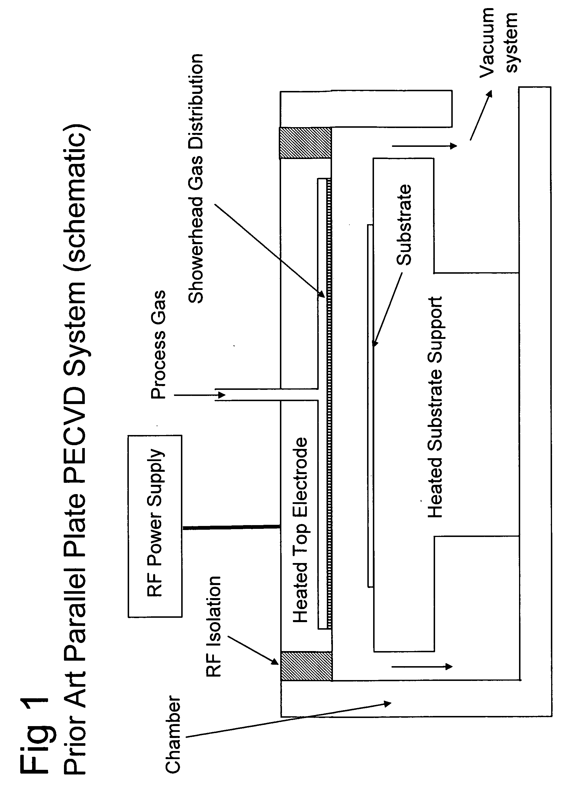
However, to be effective, the presence of this window should not locally perturb the plasma, since this will affect the area of the substrate which is being monitored.
The light pipe used to collect the plasma emission intrudes into, and hence disturbs, the plasma.
Also, no provision is made to prevent degradation of the optical components over time due to the etch process.
This necessitates a large (50 mm) window, which is acceptable for the etch applications discussed, but is unacceptable for a parallel plate PECVD application.
Chen et al. do not teach placing the window within an electrode and the configuration is not applicable to a parallel plate PECVD system.

Method used


Image

  • Optical emission interferometry for PECVD using a gas injection hole
  • Optical emission interferometry for PECVD using a gas injection hole
  • Optical emission interferometry for PECVD using a gas injection hole

Examples


examples

[0054] An accurate measurement of the film thickness in real time permits the process to be terminated when a pre-determined film thickness has been achieved. This is shown in FIG. 7 where the process is terminated when a target film thickness of 7500 Å has been achieved. The deposition rate of 498.8 Å / min was determined using a linear regression analysis.

[0055] The advantage of terminating the process based on this technique over the conventional method of terminating by time is that better run to run repeatability is obtained, resulting in devices with a more consistent performance. From run to run, the deposition rate will normally change slightly due to film accumulation, which will change the reactor characteristics. Terminating a process at a fixed time inevitably results in a film thickness which also changes from run to run. Additionally, it is necessary to clean a system periodically to remove the accumulated film using a plasma clean process. After this procedure, it is u...


PUM

PropertyMeasurementUnit
Nanoscale particle sizeaaaaaaaaaa
Wavelengthaaaaaaaaaa

Abstract

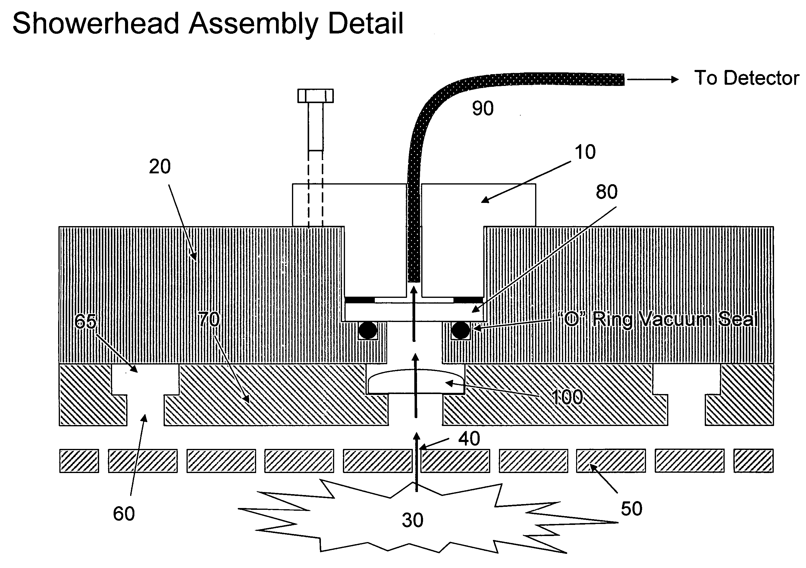
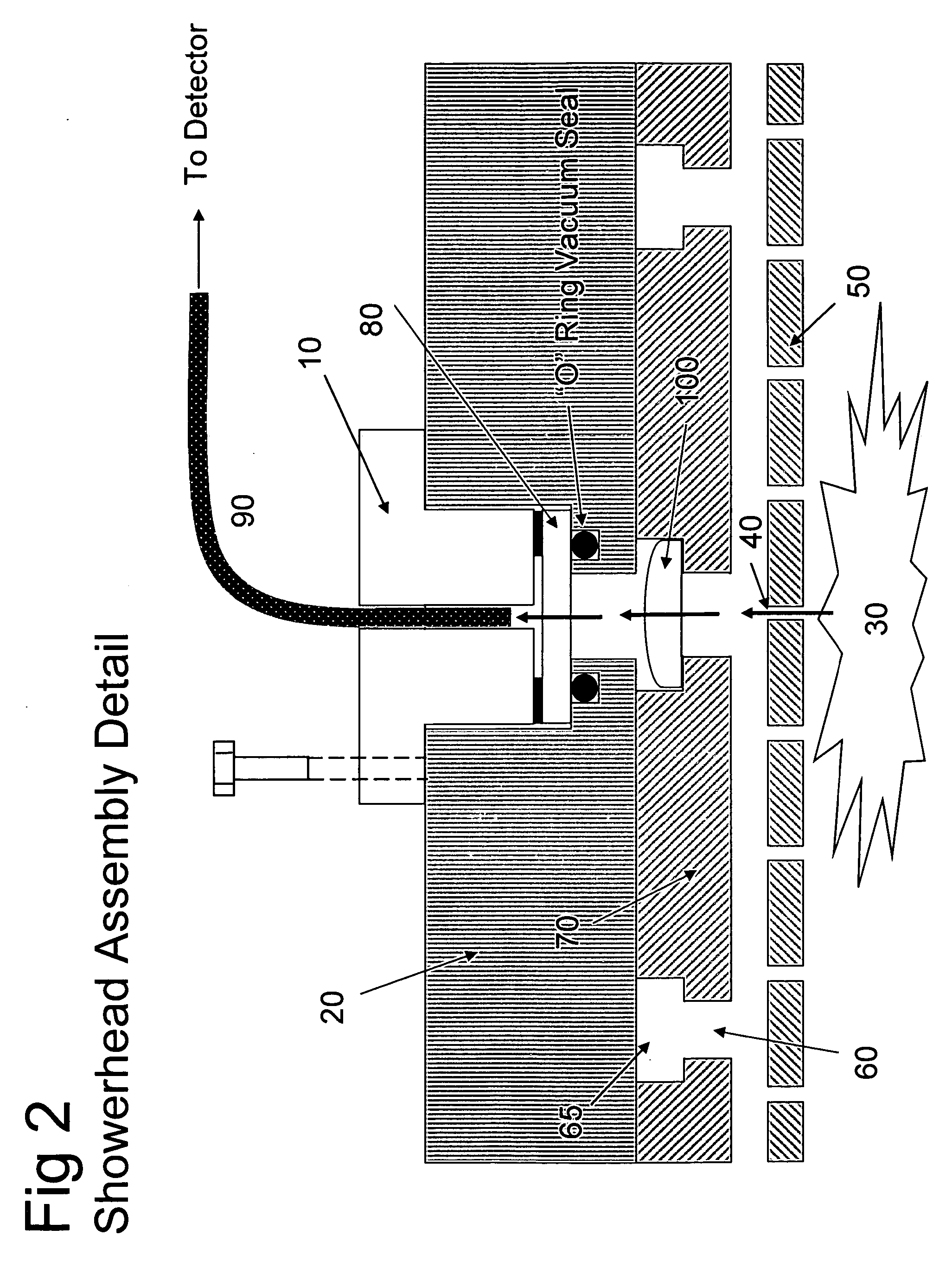
The present invention provides a method and apparatus for improving optical sensing of a plasma process through the use of a fiber optic sensor placed within a standard showerhead hole of a standard gas showerhead positioned in an upper electrode of a plasma system during the plasma processing of a substrate. A film property can be calculated based on the measured plasma emission from the surface of the substrate. The film property can be film deposition rate, refractive index, film thickness, etc. Based on the measured film property, the plasma processing of the substrate can be adjusted and / or terminated. In addition, a window is provided that is positioned in the upper electrode assembly for viewing the plasma emission through the standard showerhead hole.

Description

CROSS REFERENCES TO RELATED APPLICATIONS [0001] This application claims priority from and is related to commonly owned U.S. Provisional Patent Application Ser. No. 60 / 709,469 filed Aug. 18, 2005, entitled: Optical Emission Interferometry for PECVD using a Gas Injection Hole, this Provisional Patent Application incorporated by reference herein.FIELD OF THE INVENTION [0002] The present invention relates to plasma processing apparatus, and in particular to plasma reactor systems having an optical monitoring and control system for monitoring and controlling plasma processing. BACKGROUND [0003] Plasma processes are used extensively in the manufacture of semiconductor devices and silicon-based micro-circuits. They are also used in other non-semiconductor applications, such as waveguide and optical device fabrication and in many non silicon-based devices (devices based on III-V materials such as GaAs). [0004] Plasma processing falls into two general categories, namely etching and depositio...

Claims


Application Information

Patent Timeline
IPC IPC(8): B05C11/00
CPCC23C16/52G01B11/0658H01J37/32972H01J37/32935G01B11/0683
Inventor JOHNSON, DAVID
Owner PLASMA THERM
Learn More