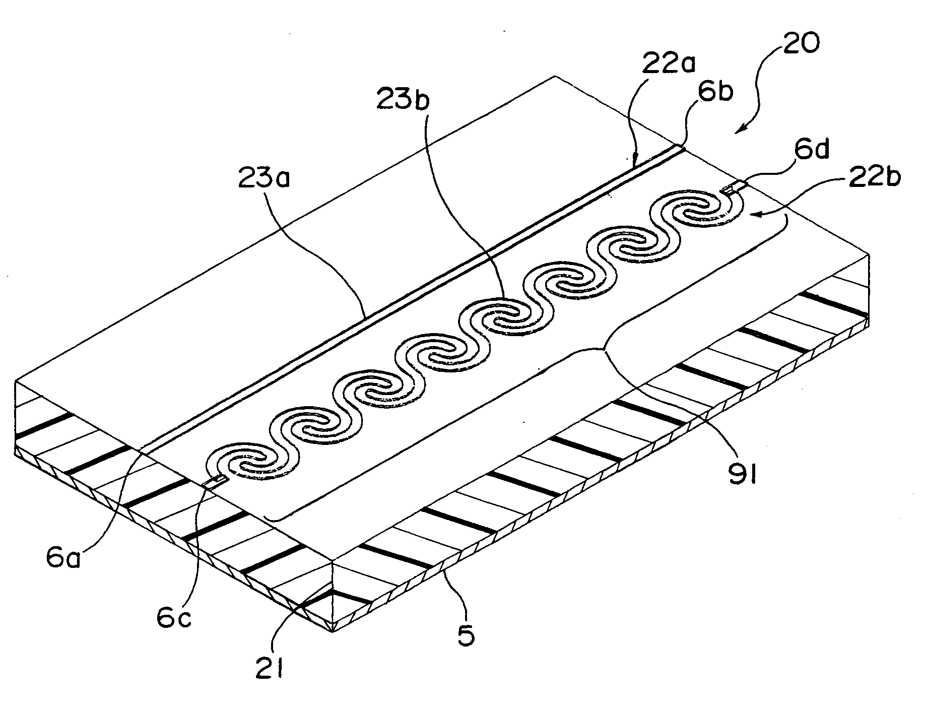
[0127] In addition, in such a transmission line, the setting for the number of spiral rotations in the rotational-direction reversal structure may be selected as an optimum value for obtainment of desired characteristics under the limitation of the circuit occupation area. For example, if the number of spiral rotations is set to within a range of about 0.5 rotation to 1.5 rotations, then the above-described effects of the invention can be obtained under a setting of the circuit occupation area, favorably. Also, in a method in which such rotational-direction reversal structure 29, 39 is adopted for the second transmission line 22b, 32b, the transmission direction of the signal to be transmitted in the second transmission line 22b, 32b can be locally led toward a direction different from the signal transmission direction in the first transmission line 22a. As a result of this, the continuity of the
current loop associated with the transmission line can be locally
cut off, the amount of
coupling with an adjacently placed transmission line due to the mutual
inductance can be reduced. That is, not only the
white noise effect for the
crosstalk signal can be obtained by the generation of an effective
dielectric constant difference, but also the
crosstalk signal intensity caused by the coupled
line structure per unit length can be suppressed. Thus, there is obtained an additional effect that not only spike
noise sharper is dissipated in the crosstalk waveform to make the waveform into
white noise, but also the intensity of the crosstalk signal can be effectively suppressed.
[0128] As shown in FIG. 4B, in the rotational-direction reversal structure 29 of the second transmission line 22b, the transmission-direction reversal section (transmission-direction reversal region or transmission-direction reversal structural portion) 97 for locally transmitting the signal toward a direction which differs from the signal transmission direction 96 by more than 90 degrees is included in the structure. That is, signal transmission directions in the respective first semicircular-arc structures 27a, 28a located in close proximities to the center of the rotational-direction reversal structure 29 are those differing from the transmission direction 95 by more than 90 degrees and further including a direction reversed by 180 degrees. Therefore, in the rotational-direction reversal structure 29, a structural portion formed by the first semicircular-arc structures 27a, 28a forms the transmission-direction reversal section 97.
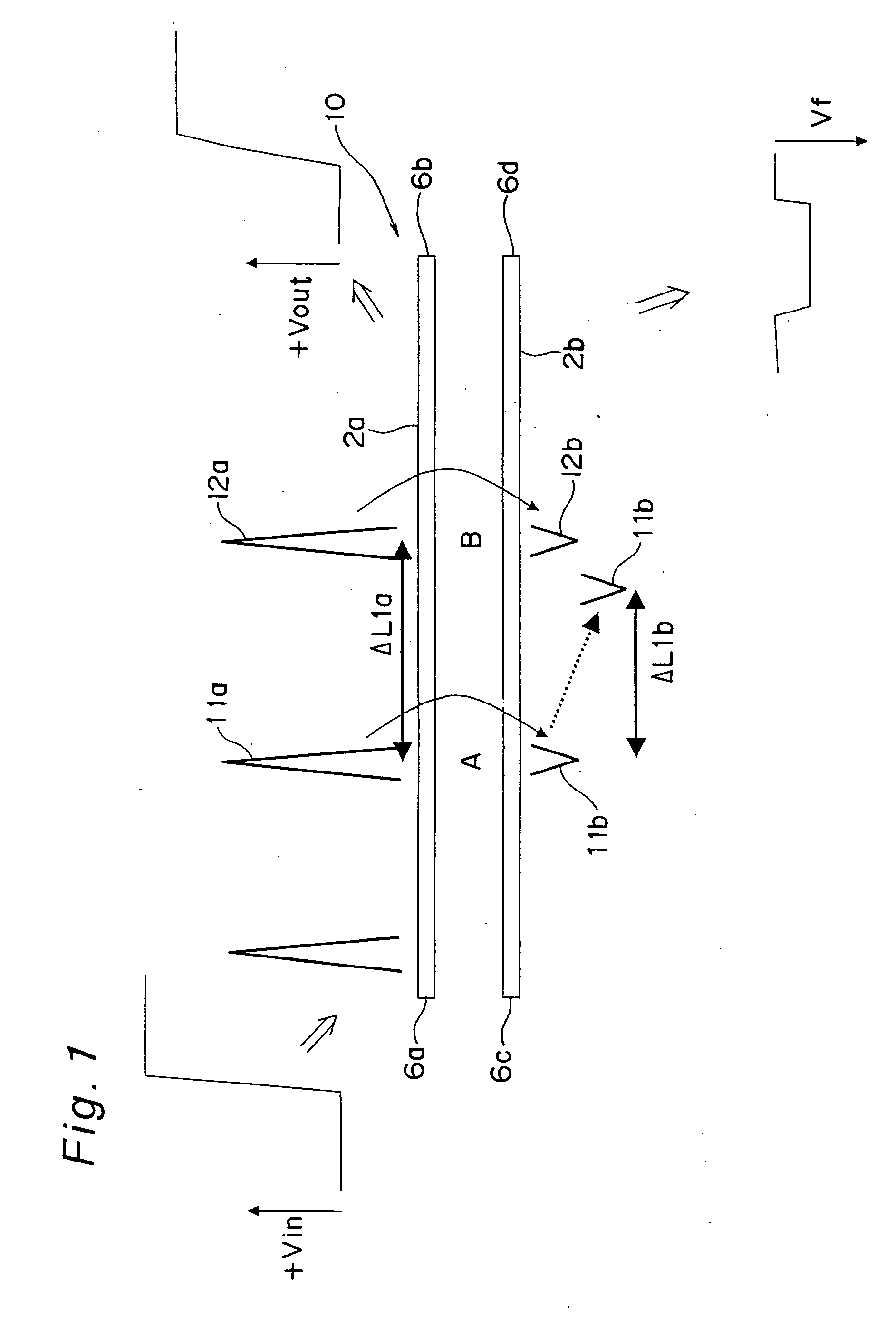
[0129] Thus, in the second transmission line 22b, in which a structure including the transmission-direction reversal section 97 is adopted, a far-end crosstalk signal generated from a signal traveling along the first transmission line 22a travels in a direction opposite to the direction of a normal far-end crosstalk signal (i.e., transmission direction 95), in the transmission-direction reversal section 97. That is, the setting of the transmission-direction reversal section 97 has a function of canceling a normal crosstalk signal. Accordingly, by the inclusion of the transmission-direction reversal section 97 in the rotational-direction reversal structure 29, the crosstalk suppression effect can be further increased. It is noted that, herein, the terms “reverse the transmission direction” refer to, in FIG. 4B, making a negative x-direction component generated in a vector in a local signal transmission direction in the transmission line, where the transmission direction 95, 96 is assumed as the X-axis direction and a direction orthogonal to this X-axis direction is assumed as the Y-axis direction.
[0130] Further, also in the rotational-direction reversal structure 39 of the second transmission line 32b shown in FIG. 5, the transmission direction of the transmitted signal is reversed by more than 90 degrees with respect to the transmission direction 95 in the first transmission line 22a, including a portion reversed up to 180 degrees, where it can be said that the transmission-direction reversal section is included. More specifically, the rotational-direction reversal structure 39 of FIG. 5 is so made up that a curved signal conductor 37 curved along the first rotational direction and a curved signal conductor 38 curved toward the second rotational direction opposite to the first rotational direction are electrically connected to each other, where the transmission-direction reversal section 97 enclosed by broken line is formed by the signal conductor in proximity to their connecting portion so that the signal transmission direction is reversed at this section. In addition, although not shown, each of the curved signal conductors 37 and 38 is formed by a combination of two types of partial circular-arc structures having different curvatures of their curves.
[0131] Further, in a transmission line pair 50 shown in FIG. 6 by a
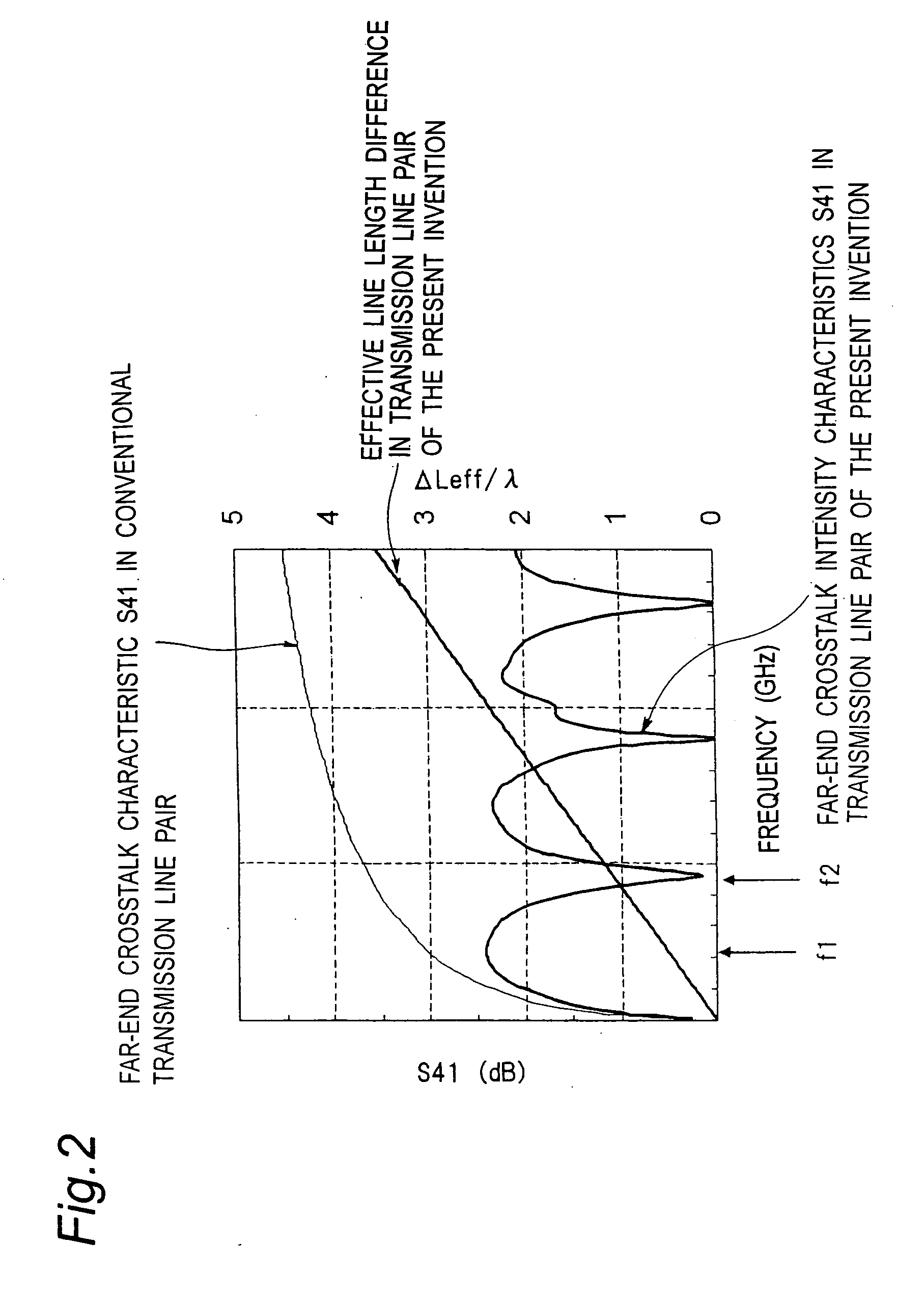
schematic perspective view, since a multiplicity of transmission-direction reversal sections 57 (partly defined and indicated by broken line) are included in the structure, so that the effect by the inclusion of the transmission-direction reversal sections 57 can be obtained more effectively. In addition, the crosstalk intensity suppression effect becomes the largest when the local signal transmission direction of the signal conductor of the second transmission line is strictly reverse to the signal transmission direction 95 (i.e., reversed by 180 degrees), which is more preferable, but the crosstalk intensity suppression effect can partly be obtained if a section having an angle more than 90 degrees to the signal transmission direction 95.
[0132] However, the placement of the signal conductor in a second transmission line 52b of FIG. 6 may cause unnecessary reflection to high-speed signals. That is, in a comparison of the structure size under the condition that the transmission line pairs 20 and 50 are equal in
line width setting to each other in FIG. 4A and FIG. 6, the effective
line length of the rotational-direction reversal structures 29 and 59 is longer in the structure of FIG. 6 than in the structure of FIG. 4A. Like this, as the effective
line length of the rotational-direction reversal structure 59 becomes longer, the
resonance frequency in the structure becomes lower, so that unfavorable phenomena such as reflection and
radiation tend to occur increasingly in frequency bands near the
resonance frequency. In order to reduce the occurrence of such unfavorable phenomena, it is preferred that the effective line length of the rotational-direction reversal structure, which is to be set in the signal conductor of the second transmission line, is so set as to be less than a half of the effective
wavelength of the transmission frequency.

