

Metal work function adjustment by ion implantation
a technology of ion implantation and metal work function, which is applied in the field of ion implantation, can solve the problems of electric field draining energy, requiring extra energy, and requiring excessively low or high voltage to be turned on or o
- Summary
- Abstract
- Description
- Claims
- Application Information
AI Technical Summary
Benefits of technology
Problems solved by technology
Method used
Image

Examples
Embodiment Construction
[0023] Ion Acceleration Type Ion Implanter System Overview
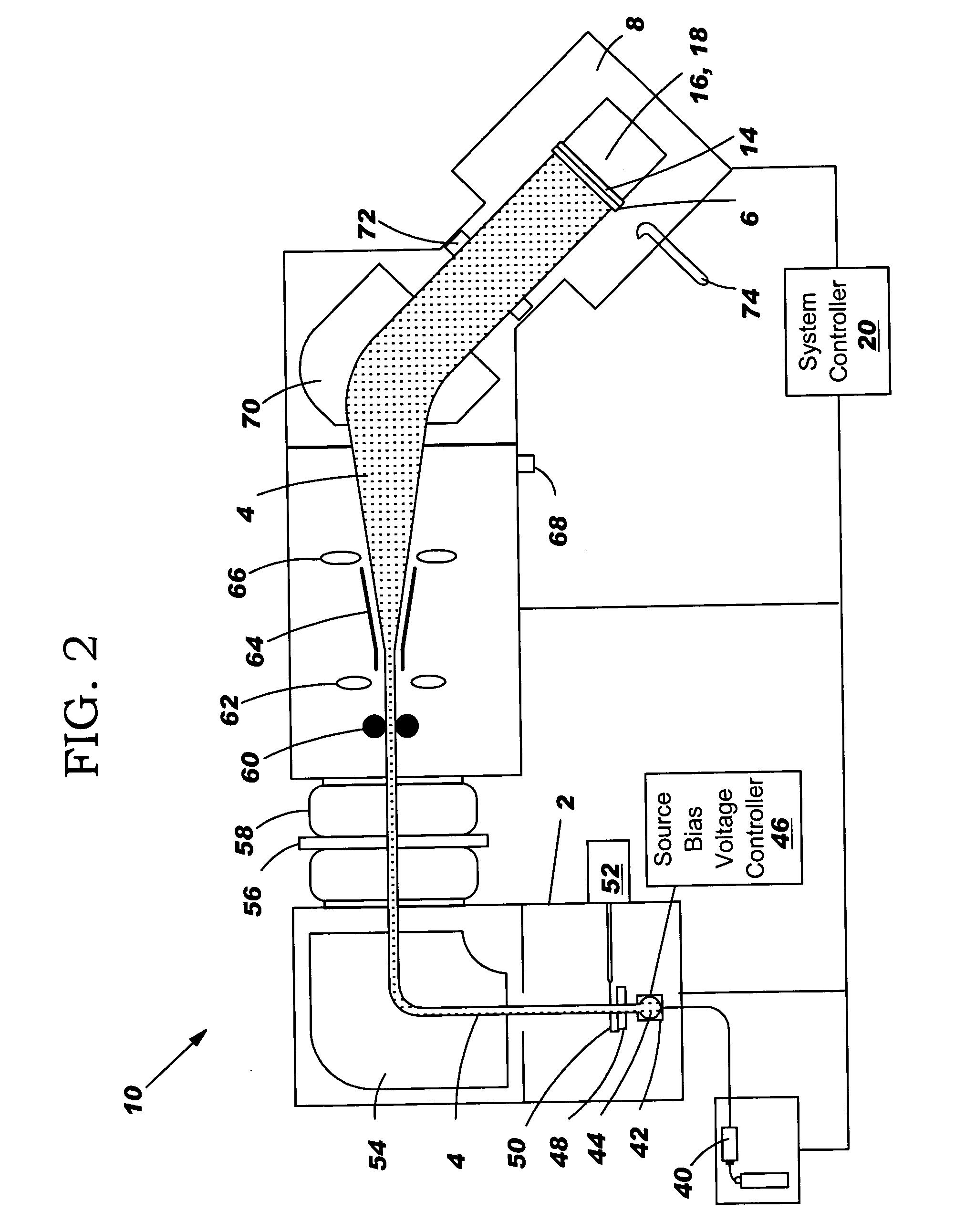
[0024] With reference to the accompanying drawings, FIG. 2 illustrates an ion acceleration type ion implanter system 10, which may be used in the present invention. Implanter system 10 includes an ion beam generator 2 for generating and transmitting an ion beam 4 to a target 6 in an implant chamber 8. Ion beam generator 2 may be any now known or later developed ion beam generator such as those available from Varian Semiconductor Equipment Associates of Gloucester, Mass. Typically, target 6 includes one or more semiconductor wafers mounted to a platen 14. Characteristics of platen 14 and, hence, target 6, may be controlled by a platen drive assembly 16 that rotates the target 6, i.e., wafer, and a target vertical scan system position controller 18 that controls the vertical position of target 6. Drive assembly 16 and position controller 18 are both responsive to a system controller 20.
[0025] Besides the above-described compo...
PUM
| Property | Measurement | Unit |
|---|---|---|
| work function | aaaaa | aaaaa |
| work function threshold | aaaaa | aaaaa |
| energy band | aaaaa | aaaaa |
Abstract
Description
Claims
Application Information