

Nitride semiconductor light-emitting device
a semiconductor and light-emitting technology, applied in semiconductor lasers, discharge tubes/lamp details, discharge tubes luminescnet screens, etc., can solve the problems of low yield rate, low defect density of substrates, and inability to meet the requirements of long useful life, etc., to achieve the effect of improving yield ra
- Summary
- Abstract
- Description
- Claims
- Application Information
AI Technical Summary
Benefits of technology
Problems solved by technology
Method used
Image

Examples
first embodiment
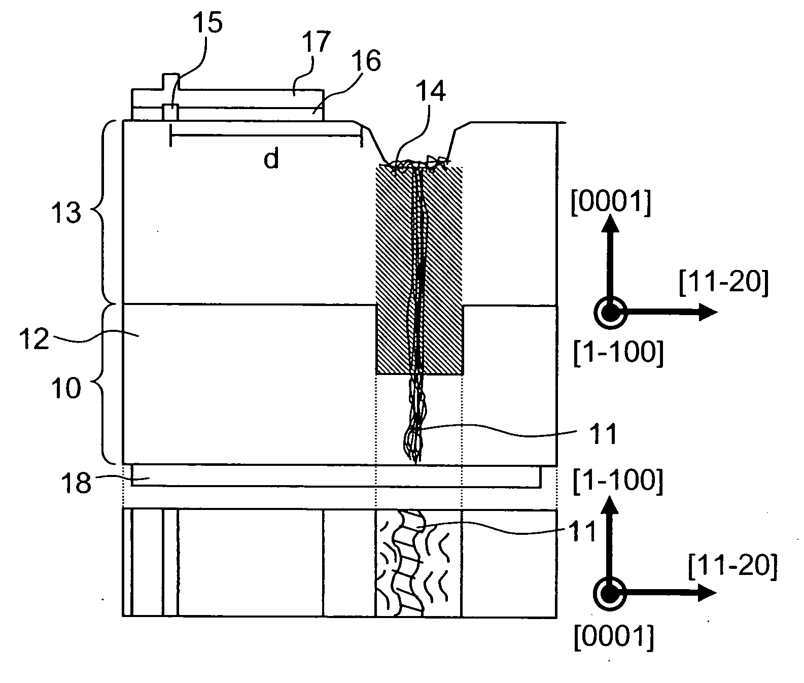
[0045]FIG. 1(a) is a sectional view of a nitride semiconductor laser device, and FIG. 1(b) is a top view of FIG. 1(a). An n-type GaN substrate 10 includes, as a part thereof, a defect-concentrated region 11, all the remaining part thereof being a low-defect region 12.
[0046] Note that, in the present specification, a defect-concentrated region denotes a region where, as a result of subjecting a substrate or a nitride semiconductor layer fabricated on a substrate to etching by dipping it in a mixed acid liquid, namely a mixture of sulfuric acid and phosphoric acid, heated to 250° C., many etch pits are observed, attesting to concentration of defects (or dislocations, for example) therein. On the other hand, a low-defect region denotes a region with EPDs (etch pit densities) of the order of 104 to 105 / cm2. The defect-concentrated region has three or more orders of magnitude greater EPDs. The measurement of the EPD can be made possible by the use of gas-phase etching such as RIE (react...
second embodiment
[0067] This embodiment deals with a case where the defect-concentrated region 11 has the shape of a dot. This embodiment has the same process and configuration, etc. as those of the first embodiment except in that, here, the defect-concentrated region 11 in the substrate 10 has the shape of a dot.
[0068] When no engraved region 14 was formed as in the conventional example described earlier, the nitride semiconductor layer 13 grew concentrically away from the defect-concentrated region 11, and the flatness in a growth meet portion was greatly degraded. We then measured the surface roughness, and observed that the level difference between the highest and lowest parts on the surface was as great as 200 nm.
[0069]FIG. 10 is a top view of the substrate 10 having the defect-concentrated region 11 in the shape of a dot. By forming the engraved region 14 in the shape of a line so as to include the dot-shaped defect-concentrated regions 11, it is possible to improve the surface flatness.
[00...
third embodiment
[0071] In this embodiment, a substrate having a depression is used. This depression may be formed elsewhere than in the defect-concentrated region 11. This embodiment has the same process and configuration, etc. as those of the first embodiment except for the substrate to be used.
[0072] The depression can take different shapes. Examples of the shape of the depression are shown in FIG. 11. FIG. 11(a) is a top view of the substrate, and FIG. 11(b) is a sectional view of FIG. 11(a). Here, assuming that these depressions 30a to 30c have the width Z and the depth V. Experiments have proved that, if the width Z is 1 μm or more and the depth V is 0.5 μm or more, the growth of the nitride semiconductor layer 13 occurs in different directions according to the shape of the depression. On the other hand, although the depression smaller and shallower than that described above is filled quickly and thus does not affect the growth direction, it degrades the surface flatness.
[0073] The region ha...
PUM
 Abstract
Description
Claims
Application Information